当前位置:
X-MOL 学术
›
Nano Lett.
›
论文详情
Our official English website, www.x-mol.net, welcomes your
feedback! (Note: you will need to create a separate account there.)
Low Residual Carrier Concentration and High Mobility in 2D Semiconducting Bi2O2Se
Nano Letters ( IF 9.6 ) Pub Date : 2018-12-17 00:00:00 , DOI: 10.1021/acs.nanolett.8b03696 Jinxiong Wu 1 , Chenguang Qiu 2 , Huixia Fu 3 , Shulin Chen 4, 5 , Congcong Zhang 1 , Zhipeng Dou 4, 5 , Congwei Tan 6 , Teng Tu 1 , Tianran Li 1 , Yichi Zhang 1 , Zhiyong Zhang 2 , Lian-Mao Peng 2 , Peng Gao 4, 5 , Binghai Yan 3 , Hailin Peng 1, 6
Nano Letters ( IF 9.6 ) Pub Date : 2018-12-17 00:00:00 , DOI: 10.1021/acs.nanolett.8b03696 Jinxiong Wu 1 , Chenguang Qiu 2 , Huixia Fu 3 , Shulin Chen 4, 5 , Congcong Zhang 1 , Zhipeng Dou 4, 5 , Congwei Tan 6 , Teng Tu 1 , Tianran Li 1 , Yichi Zhang 1 , Zhiyong Zhang 2 , Lian-Mao Peng 2 , Peng Gao 4, 5 , Binghai Yan 3 , Hailin Peng 1, 6
Affiliation
|
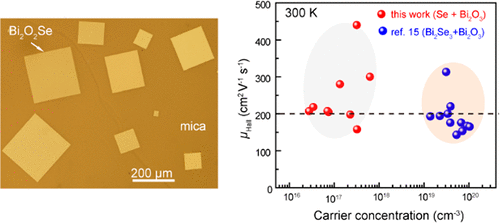
The air-stable and high-mobility two-dimensional (2D) Bi2O2Se semiconductor has emerged as a promising alternative that is complementary to graphene, MoS2, and black phosphorus for next-generation digital applications. However, the room-temperature residual charge carrier concentration of 2D Bi2O2Se nanoplates synthesized so far is as high as about 1019–1020 cm–3, which results in a poor electrostatic gate control and unsuitable threshold voltage, detrimental to the fabrication of high-performance low-power devices. Here, we first present a facile approach for synthesizing 2D Bi2O2Se single crystals with ultralow carrier concentration of ∼1016 cm–3 and high Hall mobility up to 410 cm2 V–1 s–1 simultaneously at room temperature. With optimized conditions, these high-mobility and low-carrier-concentration 2D Bi2O2Se nanoplates with domain sizes greater than 250 μm and thicknesses down to 4 layers (∼2.5 nm) were readily grown by using Se and Bi2O3 powders as coevaporation sources in a dual heating zone chemical vapor deposition (CVD) system. High-quality 2D Bi2O2Se crystals were fabricated into high-performance and low-power transistors, showing excellent current modulation of >106, robust current saturation, and low threshold voltage of −0.4 V. All these features suggest 2D Bi2O2Se as an alternative option for high-performance low-power digital applications.
中文翻译:

二维半导体Bi 2 O 2 Se的低残留载流子浓度和高迁移率
空气稳定且高迁移率的二维(2D)Bi 2 O 2 Se半导体已成为一种有前途的替代品,可替代石墨烯,MoS 2和黑磷用于下一代数字应用。但是,到目前为止合成的2D Bi 2 O 2 Se纳米板的室温残余电荷载流子浓度高达10 19 –10 20 cm –3左右,这导致静电栅极控制差和阈值电压不合适,不利于高性能低功耗设备的制造。在这里,我们首先提出一种简便的方法来合成2D Bi 2 O 2硒单晶,在室温下同时具有约10 16 cm –3的超低载流子浓度和高达410 cm 2 V –1 s –1的高霍尔迁移率。在优化的条件下,这些高迁移率和低载流子浓度的二维Bi 2 O 2 Se纳米板的畴尺寸大于250μm,厚度低至4层(〜2.5 nm),可以通过使用Se和Bi 2 O 3轻松生长。粉末在双加热区化学气相沉积(CVD)系统中作为共蒸发源。高质量2D Bi 2 O 2Se晶体被制成高性能和低功率晶体管,显示出> 10 6的出色电流调制,稳健的电流饱和和-0.4 V的低阈值电压。所有这些特征都建议使用2D Bi 2 O 2 Se作为替代选择适用于高性能低功耗数字应用。
更新日期:2018-12-17
中文翻译:
二维半导体Bi 2 O 2 Se的低残留载流子浓度和高迁移率
空气稳定且高迁移率的二维(2D)Bi 2 O 2 Se半导体已成为一种有前途的替代品,可替代石墨烯,MoS 2和黑磷用于下一代数字应用。但是,到目前为止合成的2D Bi 2 O 2 Se纳米板的室温残余电荷载流子浓度高达10 19 –10 20 cm –3左右,这导致静电栅极控制差和阈值电压不合适,不利于高性能低功耗设备的制造。在这里,我们首先提出一种简便的方法来合成2D Bi 2 O 2硒单晶,在室温下同时具有约10 16 cm –3的超低载流子浓度和高达410 cm 2 V –1 s –1的高霍尔迁移率。在优化的条件下,这些高迁移率和低载流子浓度的二维Bi 2 O 2 Se纳米板的畴尺寸大于250μm,厚度低至4层(〜2.5 nm),可以通过使用Se和Bi 2 O 3轻松生长。粉末在双加热区化学气相沉积(CVD)系统中作为共蒸发源。高质量2D Bi 2 O 2Se晶体被制成高性能和低功率晶体管,显示出> 10 6的出色电流调制,稳健的电流饱和和-0.4 V的低阈值电压。所有这些特征都建议使用2D Bi 2 O 2 Se作为替代选择适用于高性能低功耗数字应用。


 京公网安备 11010802027423号