Our official English website, www.x-mol.net, welcomes your
feedback! (Note: you will need to create a separate account there.)
Towards high-bandwidth organic photodetection based on pure active layer polarization.
Scientific Reports ( IF 3.8 ) Pub Date : 2018-Oct-18 , DOI: 10.1038/s41598-018-33822-z
Louisa Reissig , Simon Dalgleish , Kunio Awaga
Scientific Reports ( IF 3.8 ) Pub Date : 2018-Oct-18 , DOI: 10.1038/s41598-018-33822-z
Louisa Reissig , Simon Dalgleish , Kunio Awaga
|
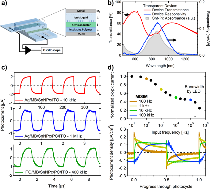
Organic photodetectors offer distinct advantages over their inorganic analogues, most notably through optical transparency and flexibility, yet their figures-of-merit still lag behind those of inorganic devices, and optimization strategies generally encounter a trade-off between device responsivity and bandwidth. Here we propose a novel photodetector architecture in which an organic photoactive semiconductor layer (S) is sandwiched between two thick insulating layers (I) that separate the semiconductor from the metallic contacts (M). In this architecture a differential photocurrent response is generated purely from the polarization of the active layer under illumination. Especially for an asymmetric MISIM design, where one insulating layer is a high-k ionic liquid IIL and the other a low-k polymer dielectric Ip, the responsivity/bandwidth trade-off is broken, since the role of the IIL in efficient charge separation is maintained, while the total device capacitance is reduced according to Ip. Thus the benefits of single insulating layer differential photodetectors (MISM) using either IIL or Ip are combined in a single device. Further improvements in device performance are also demonstrated by decreasing the series resistance of the photoactive layer through semiconductor:metal blending and by operation under strong background light.
中文翻译:

迈向基于纯有源层偏振的高带宽有机光电检测。
有机光电探测器比其无机类似物具有明显的优势,最显着的是通过光学透明性和灵活性,但是它们的品质因数仍然落后于无机器件,并且优化策略通常会在器件响应度和带宽之间进行权衡。在这里,我们提出了一种新颖的光电探测器架构,其中有机光敏半导体层(S)夹在将半导体与金属触点(M)分开的两个厚绝缘层(I)之间。在这种架构中,仅在光照下有源层的极化会产生差分光电流响应。特别是对于不对称MISIM设计,其中一个绝缘层是高k离子液体I IL,另一绝缘层是低k聚合物电介质Ip,由于保持了I IL在有效电荷分离中的作用,而总的器件电容却根据I p减小,因此响应/带宽折衷被打破了。因此,使用I IL或I p的单绝缘层差分光电检测器(MISM)的优点被组合在单个设备中。通过降低半导体,金属混合过程中光敏层的串联电阻,以及在强背景光下操作,也证明了器件性能的进一步提高。
更新日期:2018-10-18
中文翻译:
迈向基于纯有源层偏振的高带宽有机光电检测。
有机光电探测器比其无机类似物具有明显的优势,最显着的是通过光学透明性和灵活性,但是它们的品质因数仍然落后于无机器件,并且优化策略通常会在器件响应度和带宽之间进行权衡。在这里,我们提出了一种新颖的光电探测器架构,其中有机光敏半导体层(S)夹在将半导体与金属触点(M)分开的两个厚绝缘层(I)之间。在这种架构中,仅在光照下有源层的极化会产生差分光电流响应。特别是对于不对称MISIM设计,其中一个绝缘层是高k离子液体I IL,另一绝缘层是低k聚合物电介质Ip,由于保持了I IL在有效电荷分离中的作用,而总的器件电容却根据I p减小,因此响应/带宽折衷被打破了。因此,使用I IL或I p的单绝缘层差分光电检测器(MISM)的优点被组合在单个设备中。通过降低半导体,金属混合过程中光敏层的串联电阻,以及在强背景光下操作,也证明了器件性能的进一步提高。


 京公网安备 11010802027423号