Our official English website, www.x-mol.net, welcomes your
feedback! (Note: you will need to create a separate account there.)
Integrating photonics with silicon nanoelectronics for the next generation of systems on a chip
Nature ( IF 50.5 ) Pub Date : 2018-04-01 , DOI: 10.1038/s41586-018-0028-z Amir H. Atabaki , Sajjad Moazeni , Fabio Pavanello , Hayk Gevorgyan , Jelena Notaros , Luca Alloatti , Mark T. Wade , Chen Sun , Seth A. Kruger , Huaiyu Meng , Kenaish Al Qubaisi , Imbert Wang , Bohan Zhang , Anatol Khilo , Christopher V. Baiocco , Miloš A. Popović , Vladimir M. Stojanović , Rajeev J. Ram
Nature ( IF 50.5 ) Pub Date : 2018-04-01 , DOI: 10.1038/s41586-018-0028-z Amir H. Atabaki , Sajjad Moazeni , Fabio Pavanello , Hayk Gevorgyan , Jelena Notaros , Luca Alloatti , Mark T. Wade , Chen Sun , Seth A. Kruger , Huaiyu Meng , Kenaish Al Qubaisi , Imbert Wang , Bohan Zhang , Anatol Khilo , Christopher V. Baiocco , Miloš A. Popović , Vladimir M. Stojanović , Rajeev J. Ram
|
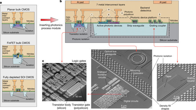
Electronic and photonic technologies have transformed our lives—from computing and mobile devices, to information technology and the internet. Our future demands in these fields require innovation in each technology separately, but also depend on our ability to harness their complementary physics through integrated solutions1,2. This goal is hindered by the fact that most silicon nanotechnologies—which enable our processors, computer memory, communications chips and image sensors—rely on bulk silicon substrates, a cost-effective solution with an abundant supply chain, but with substantial limitations for the integration of photonic functions. Here we introduce photonics into bulk silicon complementary metal–oxide–semiconductor (CMOS) chips using a layer of polycrystalline silicon deposited on silicon oxide (glass) islands fabricated alongside transistors. We use this single deposited layer to realize optical waveguides and resonators, high-speed optical modulators and sensitive avalanche photodetectors. We integrated this photonic platform with a 65-nanometre-transistor bulk CMOS process technology inside a 300-millimetre-diameter-wafer microelectronics foundry. We then implemented integrated high-speed optical transceivers in this platform that operate at ten gigabits per second, composed of millions of transistors, and arrayed on a single optical bus for wavelength division multiplexing, to address the demand for high-bandwidth optical interconnects in data centres and high-performance computing3,4. By decoupling the formation of photonic devices from that of transistors, this integration approach can achieve many of the goals of multi-chip solutions5, but with the performance, complexity and scalability of ‘systems on a chip’1,6–8. As transistors smaller than ten nanometres across become commercially available9, and as new nanotechnologies emerge10,11, this approach could provide a way to integrate photonics with state-of-the-art nanoelectronics.A way of integrating photonics with silicon nanoelectronics is described, using polycrystalline silicon on glass islands alongside transistors on bulk silicon complementary metal–oxide–semiconductor chips.
中文翻译:

将光子学与硅纳米电子学集成到下一代片上系统中
电子和光子技术改变了我们的生活——从计算和移动设备,到信息技术和互联网。我们在这些领域的未来需求需要分别对每项技术进行创新,但也取决于我们通过集成解决方案利用其互补物理的能力1,2。由于大多数硅纳米技术(使我们的处理器、计算机存储器、通信芯片和图像传感器成为可能)依赖于块状硅衬底,这是一种具有丰富供应链的经济高效的解决方案,但在集成方面存在很大限制,这一事实阻碍了这一目标光子函数。在这里,我们使用沉积在与晶体管一起制造的氧化硅(玻璃)岛上的多晶硅层将光子学引入体硅互补金属氧化物半导体(CMOS)芯片。我们使用这个单一的沉积层来实现光波导和谐振器、高速光调制器和灵敏的雪崩光电探测器。我们在直径 300 毫米的晶圆微电子代工厂中将此光子平台与 65 纳米晶体管体 CMOS 工艺技术集成在一起。然后,我们在这个平台中实现了集成高速光收发器,其运行速度为 10 Gb/s,由数百万个晶体管组成,并排列在单个光总线上进行波分复用,以满足数据中心和高性能计算对高带宽光互连的需求3,4。通过将光子器件的形成与晶体管的形成分离,这种集成方法可以实现多芯片解决方案的许多目标 5,但具有“片上系统”1,6-8 的性能、复杂性和可扩展性。随着直径小于 10 纳米的晶体管上市9,以及随着新纳米技术的出现10、11,这种方法可以提供一种将光子学与最先进的纳米电子学集成的方法。描述了一种将光子学与硅纳米电子学集成的方法,使用玻璃岛上的多晶硅与体硅互补金属氧化物半导体芯片上的晶体管。通过将光子器件的形成与晶体管的形成分离,这种集成方法可以实现多芯片解决方案的许多目标 5,但具有“片上系统”1,6-8 的性能、复杂性和可扩展性。随着直径小于 10 纳米的晶体管上市9,以及随着新纳米技术的出现10、11,这种方法可以提供一种将光子学与最先进的纳米电子学集成的方法。描述了一种将光子学与硅纳米电子学集成的方法,使用玻璃岛上的多晶硅与体硅互补金属氧化物半导体芯片上的晶体管。通过将光子器件的形成与晶体管的形成分离,这种集成方法可以实现多芯片解决方案的许多目标 5,但具有“片上系统”1,6-8 的性能、复杂性和可扩展性。随着直径小于 10 纳米的晶体管上市9,以及随着新纳米技术的出现10、11,这种方法可以提供一种将光子学与最先进的纳米电子学集成的方法。描述了一种将光子学与硅纳米电子学集成的方法,使用玻璃岛上的多晶硅与体硅互补金属氧化物半导体芯片上的晶体管。
更新日期:2018-04-01
中文翻译:
将光子学与硅纳米电子学集成到下一代片上系统中
电子和光子技术改变了我们的生活——从计算和移动设备,到信息技术和互联网。我们在这些领域的未来需求需要分别对每项技术进行创新,但也取决于我们通过集成解决方案利用其互补物理的能力1,2。由于大多数硅纳米技术(使我们的处理器、计算机存储器、通信芯片和图像传感器成为可能)依赖于块状硅衬底,这是一种具有丰富供应链的经济高效的解决方案,但在集成方面存在很大限制,这一事实阻碍了这一目标光子函数。在这里,我们使用沉积在与晶体管一起制造的氧化硅(玻璃)岛上的多晶硅层将光子学引入体硅互补金属氧化物半导体(CMOS)芯片。我们使用这个单一的沉积层来实现光波导和谐振器、高速光调制器和灵敏的雪崩光电探测器。我们在直径 300 毫米的晶圆微电子代工厂中将此光子平台与 65 纳米晶体管体 CMOS 工艺技术集成在一起。然后,我们在这个平台中实现了集成高速光收发器,其运行速度为 10 Gb/s,由数百万个晶体管组成,并排列在单个光总线上进行波分复用,以满足数据中心和高性能计算对高带宽光互连的需求3,4。通过将光子器件的形成与晶体管的形成分离,这种集成方法可以实现多芯片解决方案的许多目标 5,但具有“片上系统”1,6-8 的性能、复杂性和可扩展性。随着直径小于 10 纳米的晶体管上市9,以及随着新纳米技术的出现10、11,这种方法可以提供一种将光子学与最先进的纳米电子学集成的方法。描述了一种将光子学与硅纳米电子学集成的方法,使用玻璃岛上的多晶硅与体硅互补金属氧化物半导体芯片上的晶体管。通过将光子器件的形成与晶体管的形成分离,这种集成方法可以实现多芯片解决方案的许多目标 5,但具有“片上系统”1,6-8 的性能、复杂性和可扩展性。随着直径小于 10 纳米的晶体管上市9,以及随着新纳米技术的出现10、11,这种方法可以提供一种将光子学与最先进的纳米电子学集成的方法。描述了一种将光子学与硅纳米电子学集成的方法,使用玻璃岛上的多晶硅与体硅互补金属氧化物半导体芯片上的晶体管。通过将光子器件的形成与晶体管的形成分离,这种集成方法可以实现多芯片解决方案的许多目标 5,但具有“片上系统”1,6-8 的性能、复杂性和可扩展性。随着直径小于 10 纳米的晶体管上市9,以及随着新纳米技术的出现10、11,这种方法可以提供一种将光子学与最先进的纳米电子学集成的方法。描述了一种将光子学与硅纳米电子学集成的方法,使用玻璃岛上的多晶硅与体硅互补金属氧化物半导体芯片上的晶体管。


 京公网安备 11010802027423号