当前位置:
X-MOL 学术
›
ACS Appl. Mater. Interfaces
›
论文详情
Our official English website, www.x-mol.net, welcomes your
feedback! (Note: you will need to create a separate account there.)
Characteristics of an Amorphous Carbon Layer as a Diffusion Barrier for an Advanced Copper Interconnect.
ACS Applied Materials & Interfaces ( IF 8.3 ) Pub Date : 2019-12-31 , DOI: 10.1021/acsami.9b15562 Byeong-Seon An 1 , Yena Kwon 1 , Jin-Su Oh 1 , Changmin Lee 1 , Seongheum Choi 1 , Hyoungsub Kim 1 , Miji Lee 2 , Sangwoo Pae 2 , Cheol-Woong Yang 1
ACS Applied Materials & Interfaces ( IF 8.3 ) Pub Date : 2019-12-31 , DOI: 10.1021/acsami.9b15562 Byeong-Seon An 1 , Yena Kwon 1 , Jin-Su Oh 1 , Changmin Lee 1 , Seongheum Choi 1 , Hyoungsub Kim 1 , Miji Lee 2 , Sangwoo Pae 2 , Cheol-Woong Yang 1
Affiliation
|
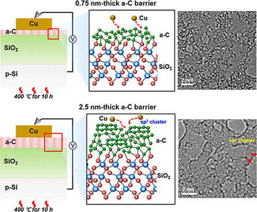
The size of the advanced Cu interconnects has been significantly reduced, reaching the current 7.0 nm node technology and below. With the relentless scaling-down of microelectronic devices, the advanced Cu interconnects thus requires an ultrathin and reliable diffusion barrier layer to prevent Cu diffusion into the surrounding dielectric. In this paper, amorphous carbon (a-C) layers of 0.75-2.5 nm thickness have been studied for use as copper diffusion barriers. The barrier performance and thermal stability of the a-C layers were evaluated by annealing Cu/SiO2/Si metal-oxide-semiconductor (MOS) samples with and without an a-C diffusion barrier at 400 °C for 10 h. Microstructure and elemental analysis performed by transmission electron microscopy (TEM) and secondary ion mass spectroscopy showed that no Cu diffusion into the SiO2 layer occurred in the presence of the a-C barrier layer. However, current density-electric field and capacitance-voltage measurements showed that 0.75 and 2.5 nm thick a-C barriers behave differently because of different microstructures being formed in each thickness after annealing. The presence of the 0.75 nm thick a-C barrier layer considerably improved the reliability of the fabricated MOS samples. In contrast, the reliability of MOS samples with a 2.5 nm thick a-C barrier was degraded by sp2 clustering and microstructural change from amorphous phase to nanocrystalline state during annealing. These results were confirmed by Raman spectroscopy, X-ray photoelectron spectroscopy and TEM analysis. This study provides evidence that an 0.75 nm thick a-C layer is a reliable diffusion barrier.
中文翻译:

非晶碳层作为高级铜互连的扩散阻挡层的特性。
先进的Cu互连的尺寸已大大减小,达到了目前的7.0 nm及以下的节点技术。随着微电子器件的不断缩小,先进的铜互连因此需要超薄且可靠的扩散阻挡层,以防止铜扩散到周围的电介质中。在本文中,已经研究了厚度为0.75-2.5 nm的非晶碳(aC)层用作铜扩散阻挡层。通过在400°C和无aC扩散阻挡层的条件下对Cu / SiO2 / Si金属氧化物半导体(MOS)样品进行退火10小时,评估了aC层的阻挡性能和热稳定性。通过透射电子显微镜(TEM)和二次离子质谱进行的微观结构和元素分析表明,在存在aC阻挡层的情况下,没有Cu扩散到SiO2层中。然而,电流密度-电场和电容-电压测量结果表明,由于退火后在每个厚度中形成不同的微观结构,因此0.75和2.5 nm厚的aC势垒的行为不同。0.75 nm厚的aC势垒层的存在大大提高了所制造MOS样品的可靠性。相比之下,退火过程中,sp2簇和从非晶态到纳米晶态的微观结构变化会降低具有2.5 nm厚aC势垒的MOS样品的可靠性。这些结果通过拉曼光谱法得到证实,X射线光电子能谱和TEM分析。这项研究提供了证据,证明0.75 nm厚的aC层是可靠的扩散阻挡层。
更新日期:2019-12-31
中文翻译:
非晶碳层作为高级铜互连的扩散阻挡层的特性。
先进的Cu互连的尺寸已大大减小,达到了目前的7.0 nm及以下的节点技术。随着微电子器件的不断缩小,先进的铜互连因此需要超薄且可靠的扩散阻挡层,以防止铜扩散到周围的电介质中。在本文中,已经研究了厚度为0.75-2.5 nm的非晶碳(aC)层用作铜扩散阻挡层。通过在400°C和无aC扩散阻挡层的条件下对Cu / SiO2 / Si金属氧化物半导体(MOS)样品进行退火10小时,评估了aC层的阻挡性能和热稳定性。通过透射电子显微镜(TEM)和二次离子质谱进行的微观结构和元素分析表明,在存在aC阻挡层的情况下,没有Cu扩散到SiO2层中。然而,电流密度-电场和电容-电压测量结果表明,由于退火后在每个厚度中形成不同的微观结构,因此0.75和2.5 nm厚的aC势垒的行为不同。0.75 nm厚的aC势垒层的存在大大提高了所制造MOS样品的可靠性。相比之下,退火过程中,sp2簇和从非晶态到纳米晶态的微观结构变化会降低具有2.5 nm厚aC势垒的MOS样品的可靠性。这些结果通过拉曼光谱法得到证实,X射线光电子能谱和TEM分析。这项研究提供了证据,证明0.75 nm厚的aC层是可靠的扩散阻挡层。


 京公网安备 11010802027423号