当前位置:
X-MOL 学术
›
J. Phys. Chem. Lett.
›
论文详情
Our official English website, www.x-mol.net, welcomes your
feedback! (Note: you will need to create a separate account there.)
Few-Layer PbI2 Nanoparticle: A 2D Semiconductor with Lateral Quantum Confinement.
The Journal of Physical Chemistry Letters ( IF 4.8 ) Pub Date : 2019-12-06 , DOI: 10.1021/acs.jpclett.9b03009 Jinqiu Liu 1 , Yan Sun 2 , Yong Zhou 1 , Chunfeng Zhang 1 , Xiaoyong Wang 1 , Lin Wang 2 , Min Xiao 1, 3
The Journal of Physical Chemistry Letters ( IF 4.8 ) Pub Date : 2019-12-06 , DOI: 10.1021/acs.jpclett.9b03009 Jinqiu Liu 1 , Yan Sun 2 , Yong Zhou 1 , Chunfeng Zhang 1 , Xiaoyong Wang 1 , Lin Wang 2 , Min Xiao 1, 3
Affiliation
|
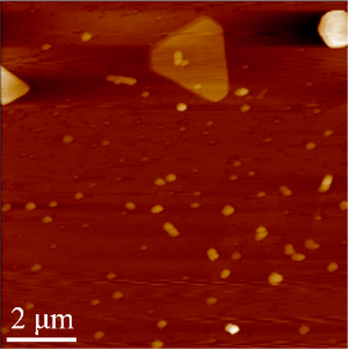
Inspired by the superior optoelectronic performances of various 2D semiconductors, their new compositions and structures are being actively pursued in order to foster novel fundamental physics and device applications. As a layered semiconductor with a direct bandgap, few-layer PbI2 should have drawn much research attention due to their capability of emitting photons at short wavelengths of the visible spectrum. Here we chemically synthesize few-layer PbI2 flakes and nanoparticles, which demonstrate unique exciton properties that have rare counterparts in other 2D semiconductors. For three layers and more, the single PbI2 flakes can be utilized to show how the bandgap energy of a 2D semiconductor evolves with the changing layer thickness. The single PbI2 nanoparticles are associated with an ultranarrow photoluminescence line width of ∼1 meV, thus reflecting the influence of lateral quantum confinement on the energy-level structures of a 2D semiconductor. The above findings mark the emergence of a potent 2D platform that is more than complementary to well-studied transition-metal dichalcogenide monolayers.
中文翻译:

少量PbI2纳米粒子:具有横向量子约束的2D半导体。
受各种2D半导体优异的光电性能的启发,人们正在积极寻求其新的成分和结构,以促进新颖的基础物理和器件应用。作为具有直接带隙的层状半导体,由于其能够在可见光谱的短波长处发射光子的能力,很少层的PbI2应该引起了很多研究关注。在这里,我们化学合成了几层的PbI2薄片和纳米颗粒,它们表现出独特的激子性质,在其他2D半导体中却很少见。对于三层或更多层,可以使用单个PbI2薄片来显示2D半导体的带隙能量如何随层厚度的变化而变化。单个的PbI2纳米粒子具有约1 meV的超窄光致发光线宽度,因此反映了横向量子限制对2D半导体能级结构的影响。以上发现标志着一个强大的二维平台的出现,该平台已与经过充分研究的过渡金属二卤化硅单分子层相辅相成。
更新日期:2019-12-07
中文翻译:
少量PbI2纳米粒子:具有横向量子约束的2D半导体。
受各种2D半导体优异的光电性能的启发,人们正在积极寻求其新的成分和结构,以促进新颖的基础物理和器件应用。作为具有直接带隙的层状半导体,由于其能够在可见光谱的短波长处发射光子的能力,很少层的PbI2应该引起了很多研究关注。在这里,我们化学合成了几层的PbI2薄片和纳米颗粒,它们表现出独特的激子性质,在其他2D半导体中却很少见。对于三层或更多层,可以使用单个PbI2薄片来显示2D半导体的带隙能量如何随层厚度的变化而变化。单个的PbI2纳米粒子具有约1 meV的超窄光致发光线宽度,因此反映了横向量子限制对2D半导体能级结构的影响。以上发现标志着一个强大的二维平台的出现,该平台已与经过充分研究的过渡金属二卤化硅单分子层相辅相成。


 京公网安备 11010802027423号