当前位置:
X-MOL 学术
›
ACS Appl. Mater. Interfaces
›
论文详情
Our official English website, www.x-mol.net, welcomes your
feedback! (Note: you will need to create a separate account there.)
Ultrahigh-Mobility and Solution-Processed Inorganic P-Channel Thin-Film Transistors Based on a Transition-Metal Halide Semiconductor
ACS Applied Materials & Interfaces ( IF 8.3 ) Pub Date : 2019-10-18 , DOI: 10.1021/acsami.9b12654 Han Ju Lee 1 , Seonjeong Lee 1 , Yena Ji 1 , Kyung Gook Cho 2 , Kyoung Soon Choi , Cheolho Jeon , Keun Hyung Lee 2 , Kihyon Hong 1
ACS Applied Materials & Interfaces ( IF 8.3 ) Pub Date : 2019-10-18 , DOI: 10.1021/acsami.9b12654 Han Ju Lee 1 , Seonjeong Lee 1 , Yena Ji 1 , Kyung Gook Cho 2 , Kyoung Soon Choi , Cheolho Jeon , Keun Hyung Lee 2 , Kihyon Hong 1
Affiliation
|
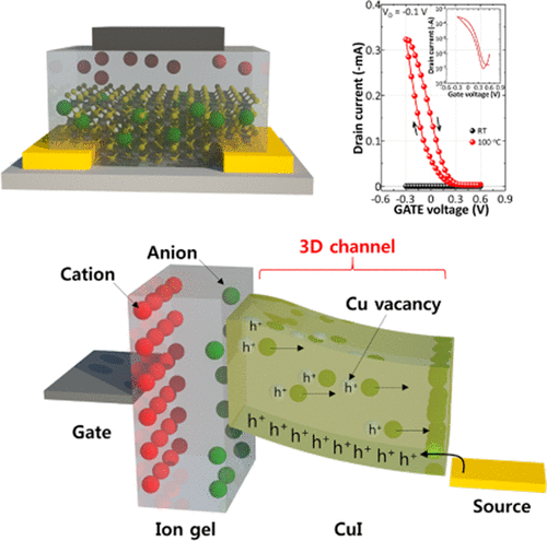
The development of p-channel devices with comparable electrical performances to their n-channel counterparts has been delayed due to the lack of p-type semiconductor materials and device optimization. In this present work, we successfully demonstrated p-channel inorganic thin-film transistors (TFTs) with high hole mobilities similar to the values of n-channel devices. To boost the device performance, the solution-processed copper iodide (CuI) semiconductor was gated by a solid polymer electrolyte. The electrolyte gating could realize electrical double layer (EDL) formation and a three-dimensional carrier transport channel and thus substantially increased charge accumulation in the channel region and realized a high mobility above 90 cm2/(V s) (45.12 ± 22.19 cm2/(V s) on average). In addition, due to the high-capacitance EDL formed by electrolyte gating, the CuI TFTs exhibited a low operation voltage below 0.5 V (Vth = −0.045 V) and a high ON current level of 0.7 mA with an ON/OFF ratio of 1.52 × 10³. We also evaluated the operational stabilities of CuI TFTs and the devices showed 80% retention under electrical/mechanical stress. All the active layers of the transistors were fabricated by solution processes at low temperatures (<100 °C), indicating their potential use for flexible, wearable, and high-performance electronic applications.
中文翻译:

基于过渡金属卤化物半导体的超高迁移率和溶液处理的无机P沟道薄膜晶体管
由于缺少p型半导体材料和器件的优化,具有与n通道同类电子性能相当的电子性能的p沟道器件的开发已被推迟。在当前的工作中,我们成功地展示了具有高空穴迁移率的p沟道无机薄膜晶体管(TFT),其与n沟道器件的值相似。为了提高器件性能,通过固态聚合物电解质对溶液处理的碘化铜(CuI)半导体进行选通。电解质门控可以实现双电层(EDL)的形成和三维载流子传输通道,从而大大增加了通道区域中的电荷积累,并在90 cm 2 /(V s)(45.12±22.19 cm 2)以上实现了高迁移率/(V s)平均)。另外,由于通过电解质门控形成的高电容EDL,CuI TFT表现出低于0.5 V(V th = -0.045 V)的低工作电压和0.7 mA的高导通电流电平,且开/关比为1.52×10 3。我们还评估了CuI TFT的操作稳定性,并且该器件在电/机械应力下显示出80%的保持力。晶体管的所有有源层都是通过低温(<100°C)的固溶工艺制造的,这表明它们在柔性,可穿戴和高性能电子应用中的潜在用途。
更新日期:2019-10-19
中文翻译:
基于过渡金属卤化物半导体的超高迁移率和溶液处理的无机P沟道薄膜晶体管
由于缺少p型半导体材料和器件的优化,具有与n通道同类电子性能相当的电子性能的p沟道器件的开发已被推迟。在当前的工作中,我们成功地展示了具有高空穴迁移率的p沟道无机薄膜晶体管(TFT),其与n沟道器件的值相似。为了提高器件性能,通过固态聚合物电解质对溶液处理的碘化铜(CuI)半导体进行选通。电解质门控可以实现双电层(EDL)的形成和三维载流子传输通道,从而大大增加了通道区域中的电荷积累,并在90 cm 2 /(V s)(45.12±22.19 cm 2)以上实现了高迁移率/(V s)平均)。另外,由于通过电解质门控形成的高电容EDL,CuI TFT表现出低于0.5 V(V th = -0.045 V)的低工作电压和0.7 mA的高导通电流电平,且开/关比为1.52×10 3。我们还评估了CuI TFT的操作稳定性,并且该器件在电/机械应力下显示出80%的保持力。晶体管的所有有源层都是通过低温(<100°C)的固溶工艺制造的,这表明它们在柔性,可穿戴和高性能电子应用中的潜在用途。


 京公网安备 11010802027423号