当前位置:
X-MOL 学术
›
J. Alloys Compd.
›
论文详情
Our official English website, www.x-mol.net, welcomes your
feedback! (Note: you will need to create a separate account there.)
Comparative study of hybrid perovskite phototransistors based on CVD-grown and spin-coated MAPbI3
Journal of Alloys and Compounds ( IF 5.8 ) Pub Date : 2020-01-01 , DOI: 10.1016/j.jallcom.2019.152404
Hyoung-Do Kim , S.V.N. Pammi , Hae-Won Lee , Sung Woo Lee , Soon-Gil Yoon , Jozeph Park , Yong Joo Kim , Hyun-Suk Kim
Journal of Alloys and Compounds ( IF 5.8 ) Pub Date : 2020-01-01 , DOI: 10.1016/j.jallcom.2019.152404
Hyoung-Do Kim , S.V.N. Pammi , Hae-Won Lee , Sung Woo Lee , Soon-Gil Yoon , Jozeph Park , Yong Joo Kim , Hyun-Suk Kim
|
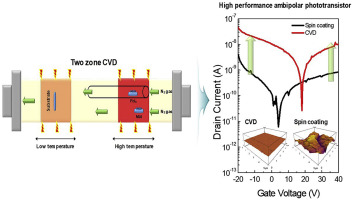
Abstract In this study, the properties of methyl ammonium lead iodide (MAPbI3) hybrid organic-inorganic perovskite films grown by spin-coating and chemical vapor deposition (CVD) method were examined and compared. Atomic force microscopy analyses indicate that the CVD-grown MAPbI3 films exhibit a smoother surface compared to their spin-coated counterparts. Phototransistors incorporating CVD-grown MAPbI3 as the active layer exhibit superior electrical characteristics, with field effect mobility values higher by approximately one order of magnitude. The degradation of phototransistors under negative bias stress (NBS) and positive bias stress (PBS) in the presence of illumination was evaluated and discussed based on the charge trapping mechanism.
中文翻译:

基于CVD生长和旋涂MAPbI3的混合钙钛矿光电晶体管的比较研究
摘要 在这项研究中,研究和比较了通过旋涂和化学气相沉积 (CVD) 方法生长的甲基碘化铅 (MAPbI3) 杂化有机-无机钙钛矿薄膜的性能。原子力显微镜分析表明,与旋涂对应物相比,CVD 生长的 MAPbI3 薄膜表现出更光滑的表面。包含 CVD 生长的 MAPbI3 作为有源层的光电晶体管表现出优异的电气特性,场效应迁移率值高出大约一个数量级。基于电荷俘获机制评估和讨论了在光照下负偏压应力 (NBS) 和正偏压应力 (PBS) 下光电晶体管的退化。
更新日期:2020-01-01
中文翻译:
基于CVD生长和旋涂MAPbI3的混合钙钛矿光电晶体管的比较研究
摘要 在这项研究中,研究和比较了通过旋涂和化学气相沉积 (CVD) 方法生长的甲基碘化铅 (MAPbI3) 杂化有机-无机钙钛矿薄膜的性能。原子力显微镜分析表明,与旋涂对应物相比,CVD 生长的 MAPbI3 薄膜表现出更光滑的表面。包含 CVD 生长的 MAPbI3 作为有源层的光电晶体管表现出优异的电气特性,场效应迁移率值高出大约一个数量级。基于电荷俘获机制评估和讨论了在光照下负偏压应力 (NBS) 和正偏压应力 (PBS) 下光电晶体管的退化。


 京公网安备 11010802027423号