当前位置:
X-MOL 学术
›
J. Mater. Chem. C
›
论文详情
Our official English website, www.x-mol.net, welcomes your
feedback! (Note: you will need to create a separate account there.)
High-performance UV detectors based on room-temperature deposited amorphous Ga2O3 thin films by RF magnetron sputtering
Journal of Materials Chemistry C ( IF 5.7 ) Pub Date : 2019-08-26 , DOI: 10.1039/c9tc03613j Shun Han 1, 2, 3, 4, 5 , Xiaoling Huang 1, 2, 3, 4, 5 , Mingzhi Fang 1, 2, 3, 4, 5 , Weiguo Zhao 1, 2, 3, 4, 5 , Shijie Xu 6, 7, 8 , Deliang Zhu 1, 2, 3, 4, 5 , Wangying Xu 1, 2, 3, 4, 5 , Ming Fang 1, 2, 3, 4, 5 , Wenjun Liu 1, 2, 3, 4, 5 , Peijiang Cao 1, 2, 3, 4, 5 , Youming Lu 1, 2, 3, 4, 5
Journal of Materials Chemistry C ( IF 5.7 ) Pub Date : 2019-08-26 , DOI: 10.1039/c9tc03613j Shun Han 1, 2, 3, 4, 5 , Xiaoling Huang 1, 2, 3, 4, 5 , Mingzhi Fang 1, 2, 3, 4, 5 , Weiguo Zhao 1, 2, 3, 4, 5 , Shijie Xu 6, 7, 8 , Deliang Zhu 1, 2, 3, 4, 5 , Wangying Xu 1, 2, 3, 4, 5 , Ming Fang 1, 2, 3, 4, 5 , Wenjun Liu 1, 2, 3, 4, 5 , Peijiang Cao 1, 2, 3, 4, 5 , Youming Lu 1, 2, 3, 4, 5
Affiliation
|
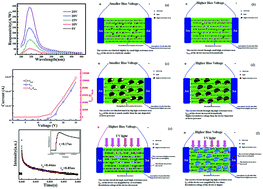
Room-temperature-fabricated amorphous Ga2O3 is an inexpensive and highly sensitive material for high-performance solar-blind ultraviolet (UV) (220–280 nm) detectors, which are extremely useful given the widespread use of solar-blind UV photoelectronic technology in multiple areas. The UV detection characteristics of room-temperature deposited amorphous Ga2O3 thin films fabricated by a simple RF magnetron sputtering method were studied, and the deposition Ar pressure of an a-Ga2O3 thin film was varied to determine the mechanism underlying high-performance UV detection and to develop an ideal a-Ga2O3 thin film for UV detection. A high-response amorphous Ga2O3-based UV detector was made at 0.5 Pa, and the maximum response of the device reached 436.3 A W−1 under 240 nm UV light with a 25 V bias voltage, which is near the maximum values for a single-crystal β-Ga2O3 material deposited at a high temperature. An amorphous Ga2O3-based UV detector with a low Idark noise level (4.9 nA at 25 V) and a high Iuv/Idark ratio (107314.4) was made at 1.2 Pa, and the Iuv/Idark ratio of the device was near that of a UV detector based on single-crystal β-Ga2O3 with a complex metal-oxide–semiconductor field-effect transistor (MOSFET) structure. Through a comparative analysis of the electrical characteristics and the gain mechanism within amorphous Ga2O3 thin films deposited at different Ar pressures, the high UV response of the amorphous Ga2O3 detector at 0.5 Pa is found to mainly result from the quasi-Zener tunneling multiplication phenomenon between different resistance components. The low Idark value and the high signal-to-noise ratio of the amorphous Ga2O3-based detector deposited at 1.2 Pa were mainly due to more high-resistance components and a relatively higher tunneling gain in the device. In addition, the amorphous Ga2O3-based detectors showed a much shorter response time (0.08 μs for the device deposited at 0.65 Pa) and recovery time (td1 = 0.21 ms, td2 = 5.88 ms for the device deposited at 1.2 Pa) than the reported crystal semiconductor-based devices and multiple complex structure devices. Thus, the room-temperature-fabricated amorphous Ga2O3 thin film could quickly and effectively detect a faint UV light signal in the presence of a very noisy background, which is extremely important in the applications of UV detectors in wearable, flexible photoelectronic devices.
中文翻译:

基于射频磁控溅射的室温沉积非晶Ga 2 O 3薄膜 的高性能紫外线检测器
室温制造的非晶态Ga 2 O 3是一种廉价且高度灵敏的材料,适用于高性能太阳盲紫外线(UV)(220-280 nm)检测器,鉴于太阳盲UV光电电子的广泛使用,这种材料非常有用多个领域的技术。研究了通过简单的射频磁控溅射法制备的室温沉积非晶态Ga 2 O 3薄膜的紫外检测特性,并改变了a-Ga 2 O 3薄膜的沉积Ar压力,从而确定了高温下形成非晶态Ga 2 O 3的机理。性能的紫外线检测并开发出理想的a-Ga 2 O 3用于紫外线检测的薄膜。在0.5 Pa下制作了一个高响应性,基于非晶Ga 2 O 3的UV检测器,在240 nm UV光和25 V偏置电压下,该器件的最大响应达到436.3 AW -1,接近于25 V的最大值。单晶的β-Ga 2 ö 3材料沉积在高温下。在1.2 Pa下制作了具有低I暗噪声水平(25 V时为4.9 nA)和高I uv / I暗比(107314.4)的基于Ga 2 O 3的非晶态UV检测器,I uv / I暗该装置的比为接近基于单晶的β-Ga一个UV检测器的那个2 ö 3用的复合金属氧化物半导体场效应晶体管(MOSFET)结构。通过对在不同Ar压力下沉积的非晶Ga 2 O 3薄膜中的电学特性和增益机理的比较分析,发现非晶Ga 2 O 3检测器在0.5 Pa时的高UV响应主要是由于准量子点引起的。不同电阻元件之间的齐纳隧穿倍增现象。非晶态Ga 2 O 3的低I暗值和高信噪比沉积在1.2 Pa的基于探测器的探测器主要是由于更多的高电阻组件和器件中相对较高的隧穿增益。此外,基于非晶Ga 2 O 3的检测器显示出更短的响应时间(对于在0.65 Pa下沉积的器件为0.08μs)和恢复时间(对于在1.25下沉积的器件的t d1 = 0.21 ms,t d2 = 5.88 ms Pa)比所报道的基于晶体半导体的器件和多种复杂结构的器件。因此,室温制造的非晶态Ga 2 O 3 薄膜可以在非常嘈杂的背景下快速有效地检测到微弱的紫外线信号,这在可穿戴,柔性光电设备中紫外线检测器的应用中极为重要。
更新日期:2019-10-03
中文翻译:
基于射频磁控溅射的室温沉积非晶Ga 2 O 3薄膜 的高性能紫外线检测器
室温制造的非晶态Ga 2 O 3是一种廉价且高度灵敏的材料,适用于高性能太阳盲紫外线(UV)(220-280 nm)检测器,鉴于太阳盲UV光电电子的广泛使用,这种材料非常有用多个领域的技术。研究了通过简单的射频磁控溅射法制备的室温沉积非晶态Ga 2 O 3薄膜的紫外检测特性,并改变了a-Ga 2 O 3薄膜的沉积Ar压力,从而确定了高温下形成非晶态Ga 2 O 3的机理。性能的紫外线检测并开发出理想的a-Ga 2 O 3用于紫外线检测的薄膜。在0.5 Pa下制作了一个高响应性,基于非晶Ga 2 O 3的UV检测器,在240 nm UV光和25 V偏置电压下,该器件的最大响应达到436.3 AW -1,接近于25 V的最大值。单晶的β-Ga 2 ö 3材料沉积在高温下。在1.2 Pa下制作了具有低I暗噪声水平(25 V时为4.9 nA)和高I uv / I暗比(107314.4)的基于Ga 2 O 3的非晶态UV检测器,I uv / I暗该装置的比为接近基于单晶的β-Ga一个UV检测器的那个2 ö 3用的复合金属氧化物半导体场效应晶体管(MOSFET)结构。通过对在不同Ar压力下沉积的非晶Ga 2 O 3薄膜中的电学特性和增益机理的比较分析,发现非晶Ga 2 O 3检测器在0.5 Pa时的高UV响应主要是由于准量子点引起的。不同电阻元件之间的齐纳隧穿倍增现象。非晶态Ga 2 O 3的低I暗值和高信噪比沉积在1.2 Pa的基于探测器的探测器主要是由于更多的高电阻组件和器件中相对较高的隧穿增益。此外,基于非晶Ga 2 O 3的检测器显示出更短的响应时间(对于在0.65 Pa下沉积的器件为0.08μs)和恢复时间(对于在1.25下沉积的器件的t d1 = 0.21 ms,t d2 = 5.88 ms Pa)比所报道的基于晶体半导体的器件和多种复杂结构的器件。因此,室温制造的非晶态Ga 2 O 3 薄膜可以在非常嘈杂的背景下快速有效地检测到微弱的紫外线信号,这在可穿戴,柔性光电设备中紫外线检测器的应用中极为重要。


 京公网安备 11010802027423号