当前位置:
X-MOL 学术
›
ACS Appl. Nano Mater.
›
论文详情
Our official English website, www.x-mol.net, welcomes your
feedback! (Note: you will need to create a separate account there.)
Lead Sulfide Quantum Dot Photodetector with Enhanced Responsivity through a Two-Step Ligand-Exchange Method
ACS Applied Nano Materials ( IF 5.3 ) Pub Date : 2019-08-28 , DOI: 10.1021/acsanm.9b00889 Haodong Tang , Jialin Zhong , Wei Chen 1 , Kanming Shi 2 , Guanding Mei , Yuniu Zhang , Zuoliang Wen , Peter Müller-Buschbaum 1 , Dan Wu , Kai Wang , Xiao Wei Sun 2
ACS Applied Nano Materials ( IF 5.3 ) Pub Date : 2019-08-28 , DOI: 10.1021/acsanm.9b00889 Haodong Tang , Jialin Zhong , Wei Chen 1 , Kanming Shi 2 , Guanding Mei , Yuniu Zhang , Zuoliang Wen , Peter Müller-Buschbaum 1 , Dan Wu , Kai Wang , Xiao Wei Sun 2
Affiliation
|
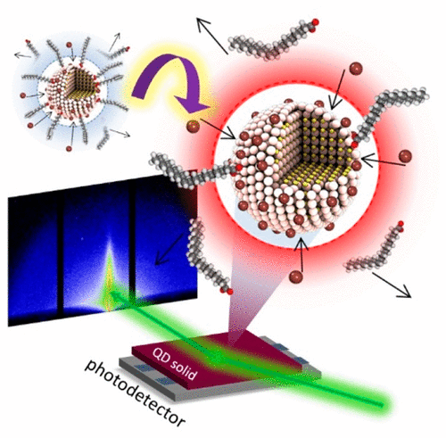
Recently, lead sulfide (PbS) quantum dots (QDs) have demonstrated great potential in becoming one of the most promising next-generation photoelectrical materials for photodetectors. PbS QDs provide fascinating properties including size-controllable spectral sensitivity, a wide and tunable absorption range, cost-efficient solution processability, and flexible substrate compatibility. One of the key problems that limit the performance of PbS QDs-based photodetectors is inefficient carrier transfer. Long ligands decorating the outside surface of PbS QDs to protect them against degeneration inhibit the transfer of electrical charge carriers and thereby limit the device performance. To overcome this problem, the long ligands need to be effectively exchanged. Here, a two-step ligand-exchange method is demonstrated. The QDs are pretreated using methylammonium iodide in solution as the first step ligand exchange before the layer-by-layer deposition process and solid-state ligand exchange. The grazing-incidence small-angle X-ray scattering and X-ray photoelectron spectroscopy analyses prove a smaller spacing among the QDs and an increased ligand-exchange ratio by adopting the two-step method. This strongly indicates a better capability of charge transfer than the traditional one-step solid-state ligand-exchange technology. Devices fabricated using the two-step method present an enhancement of the charge-transfer capability with a larger current. The efficient charge transfer is further demonstrated by a significant 94% increase of the responsivity and a 57% enhancement of the detectivity of the PbS QDs-based photodetector, reaching 3302 mA/W and 5.06 × 10¹² J, respectively.
中文翻译:

通过两步配体交换法提高响应度的硫化铅量子点光电探测器
近来,硫化铅(PbS)量子点(QDs)已显示出巨大的潜力,成为最有前途的下一代光电探测器光电材料之一。PbS QD具有引人入胜的特性,包括尺寸可控制的光谱灵敏度,宽且可调的吸收范围,经济高效的溶液可加工性以及灵活的基板兼容性。限制基于PbS QDs的光电探测器性能的关键问题之一是载流子传输效率低下。用长的配体来装饰PbS QD的外表面,以防止其退化,这会抑制电荷载流子的转移,从而限制了器件的性能。为了克服这个问题,需要有效地交换长配体。在此,说明两步的配体交换方法。在进行逐层沉积过程和固态配体交换之前,首先使用溶液中的甲基碘碘对QD进行预处理,作为第一步配体交换。掠入射小角X射线散射和X射线光电子能谱分析表明,通过采用两步法,量子点之间的间距较小,配体交换率增加。这有力地表明,电荷转移的能力比传统的一步式固态配体交换技术要好。使用两步法制造的器件在更大电流下呈现出电荷转移能力的增强。基于PbS QDs的光电探测器的响应度显着提高94%,检测率显着提高57%,达到3302 mA / W和5.06×10,进一步证明了电荷的有效转移 掠入射小角X射线散射和X射线光电子能谱分析表明,通过采用两步法,量子点之间的间距较小,配体交换率增加。这有力地表明,电荷转移的能力比传统的一步式固态配体交换技术要好。使用两步法制造的器件在更大电流下呈现出电荷转移能力的增强。基于PbS QDs的光电探测器的响应度显着提高94%,检测率显着提高57%,达到3302 mA / W和5.06×10,进一步证明了电荷的有效转移 掠入射小角X射线散射和X射线光电子能谱分析表明,通过采用两步法,量子点之间的间距较小,配体交换率增加。这有力地表明,电荷转移的能力比传统的一步式固态配体交换技术要好。使用两步法制造的器件在更大电流下呈现出电荷转移能力的增强。基于PbS QDs的光电探测器的响应度显着提高94%,检测率显着提高57%,达到了3302 mA / W和5.06×10,进一步证明了电荷的有效转移 这有力地表明,电荷转移的能力比传统的一步式固态配体交换技术要好。使用两步法制造的器件在更大电流下呈现出电荷转移能力的增强。基于PbS QDs的光电探测器的响应度显着提高94%,检测率显着提高57%,达到3302 mA / W和5.06×10,进一步证明了电荷的有效转移 这有力地表明,电荷转移的能力比传统的一步式固态配体交换技术要好。使用两步法制造的器件在更大电流下呈现出电荷转移能力的增强。基于PbS QDs的光电探测器的响应度显着提高94%,检测率显着提高57%,达到3302 mA / W和5.06×10,进一步证明了电荷的有效转移12 Ĵ,分别。
更新日期:2019-08-29
中文翻译:
通过两步配体交换法提高响应度的硫化铅量子点光电探测器
近来,硫化铅(PbS)量子点(QDs)已显示出巨大的潜力,成为最有前途的下一代光电探测器光电材料之一。PbS QD具有引人入胜的特性,包括尺寸可控制的光谱灵敏度,宽且可调的吸收范围,经济高效的溶液可加工性以及灵活的基板兼容性。限制基于PbS QDs的光电探测器性能的关键问题之一是载流子传输效率低下。用长的配体来装饰PbS QD的外表面,以防止其退化,这会抑制电荷载流子的转移,从而限制了器件的性能。为了克服这个问题,需要有效地交换长配体。在此,说明两步的配体交换方法。在进行逐层沉积过程和固态配体交换之前,首先使用溶液中的甲基碘碘对QD进行预处理,作为第一步配体交换。掠入射小角X射线散射和X射线光电子能谱分析表明,通过采用两步法,量子点之间的间距较小,配体交换率增加。这有力地表明,电荷转移的能力比传统的一步式固态配体交换技术要好。使用两步法制造的器件在更大电流下呈现出电荷转移能力的增强。基于PbS QDs的光电探测器的响应度显着提高94%,检测率显着提高57%,达到3302 mA / W和5.06×10,进一步证明了电荷的有效转移 掠入射小角X射线散射和X射线光电子能谱分析表明,通过采用两步法,量子点之间的间距较小,配体交换率增加。这有力地表明,电荷转移的能力比传统的一步式固态配体交换技术要好。使用两步法制造的器件在更大电流下呈现出电荷转移能力的增强。基于PbS QDs的光电探测器的响应度显着提高94%,检测率显着提高57%,达到3302 mA / W和5.06×10,进一步证明了电荷的有效转移 掠入射小角X射线散射和X射线光电子能谱分析表明,通过采用两步法,量子点之间的间距较小,配体交换率增加。这有力地表明,电荷转移的能力比传统的一步式固态配体交换技术要好。使用两步法制造的器件在更大电流下呈现出电荷转移能力的增强。基于PbS QDs的光电探测器的响应度显着提高94%,检测率显着提高57%,达到了3302 mA / W和5.06×10,进一步证明了电荷的有效转移 这有力地表明,电荷转移的能力比传统的一步式固态配体交换技术要好。使用两步法制造的器件在更大电流下呈现出电荷转移能力的增强。基于PbS QDs的光电探测器的响应度显着提高94%,检测率显着提高57%,达到3302 mA / W和5.06×10,进一步证明了电荷的有效转移 这有力地表明,电荷转移的能力比传统的一步式固态配体交换技术要好。使用两步法制造的器件在更大电流下呈现出电荷转移能力的增强。基于PbS QDs的光电探测器的响应度显着提高94%,检测率显着提高57%,达到3302 mA / W和5.06×10,进一步证明了电荷的有效转移12 Ĵ,分别。


 京公网安备 11010802027423号