当前位置:
X-MOL 学术
›
ACS Appl. Mater. Interfaces
›
论文详情
Our official English website, www.x-mol.net, welcomes your
feedback! (Note: you will need to create a separate account there.)
Versatile Electronic Devices Based on WSe2/SnSe2 Vertical van der Waals Heterostructures
ACS Applied Materials & Interfaces ( IF 8.3 ) Pub Date : 2019-07-25 00:00:00 , DOI: 10.1021/acsami.9b09483 Wei Li 1 , Xiang Xiao 1 , Huilong Xu 1
ACS Applied Materials & Interfaces ( IF 8.3 ) Pub Date : 2019-07-25 00:00:00 , DOI: 10.1021/acsami.9b09483 Wei Li 1 , Xiang Xiao 1 , Huilong Xu 1
Affiliation
|
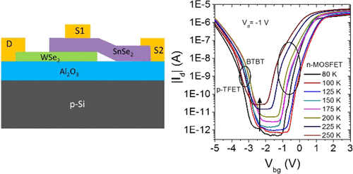
Van der Waals heterostructures formed by stacking of various two-dimensional materials are promising in electronic applications. However, the performances of most reported electronic devices based on van der Waals heterostructures are far away from those of existing (Si, Ge, and III–V bulk material based) technologies. Here, we report high-performance heterostructure devices based on vertically stacked tungsten diselenide and tin diselenide. Due to the unique band alignment and the atomic thickness of the material, both charge carrier transport and energy barrier can be effectively modulated by the applied electrical field. As a result, the heterostructure devices show superb characteristics, with a high current on/off ratio of ∼3 × 10⁸, an average subthreshold slope of 126 mV/dec over 5 dec of current change due to band-to-band tunneling, an ultrahigh rectification ratio of ∼3 × 10⁸, and a current density of more than 104 A/cm2. Furthermore, a small signal half-wave rectifier circuit based on a majority-carrier-transport-dominated diode is successfully demonstrated, showing great potential in future high-speed electronic applications.
中文翻译:

基于WSe 2 / SnSe 2垂直范德华异质结构的多功能电子设备
通过堆叠各种二维材料而形成的范德华异质结构在电子应用中很有前途。但是,大多数报告的基于范德华异质结构的电子设备的性能与现有(基于Si,Ge和III–V块状材料的)技术的性能相距甚远。在这里,我们报告了基于垂直堆叠的二硒化钨和二硒化锡的高性能异质结构器件。由于材料具有独特的能带排列和原子厚度,因此可以通过施加的电场有效地调节载流子传输和能垒。结果,异质结器件表现出了出色的特性,高的电流开/关比约为3×10 8,由于带间隧道效应,在5 dec的电流变化范围内,平均亚阈值斜率为126 mV / dec,超高整流比约为3×10 8,电流密度大于10 4 A / cm 2。此外,成功演示了基于多数载流子传输为主的二极管的小信号半波整流器电路,在未来的高速电子应用中显示出巨大的潜力。
更新日期:2019-07-25
中文翻译:
基于WSe 2 / SnSe 2垂直范德华异质结构的多功能电子设备
通过堆叠各种二维材料而形成的范德华异质结构在电子应用中很有前途。但是,大多数报告的基于范德华异质结构的电子设备的性能与现有(基于Si,Ge和III–V块状材料的)技术的性能相距甚远。在这里,我们报告了基于垂直堆叠的二硒化钨和二硒化锡的高性能异质结构器件。由于材料具有独特的能带排列和原子厚度,因此可以通过施加的电场有效地调节载流子传输和能垒。结果,异质结器件表现出了出色的特性,高的电流开/关比约为3×10 8,由于带间隧道效应,在5 dec的电流变化范围内,平均亚阈值斜率为126 mV / dec,超高整流比约为3×10 8,电流密度大于10 4 A / cm 2。此外,成功演示了基于多数载流子传输为主的二极管的小信号半波整流器电路,在未来的高速电子应用中显示出巨大的潜力。


 京公网安备 11010802027423号