Light: Science & Applications ( IF 20.6 ) Pub Date : 2019-07-24 , DOI: 10.1038/s41377-019-0178-2 Zhi-Bin Fan , Hao-Yang Qiu , Han-Le Zhang , Xiao-Ning Pang , Li-Dan Zhou , Lin Liu , Hui Ren , Qiong-Hua Wang , Jian-Wen Dong
|
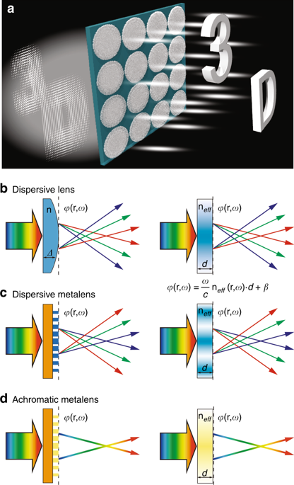
Integral imaging is a promising three-dimensional (3D) imaging technique that captures and reconstructs light field information. Microlens arrays are usually used for the reconstruction process to display 3D scenes to the viewer. However, the inherent chromatic aberration of the microlens array reduces the viewing quality, and thus, broadband achromatic imaging remains a challenge for integral imaging. Here, we realize a silicon nitride metalens array in the visible region that can be used to reconstruct 3D optical scenes in the achromatic integral imaging for white light. The metalens array contains 60 × 60 polarization-insensitive metalenses with nearly diffraction-limited focusing. The nanoposts in each high-efficiency (measured as 47% on average) metalens are delicately designed with zero effective material dispersion and an effective achromatic refractive index distribution from 430 to 780 nm. In addition, such an achromatic metalens array is composed of only a single silicon nitride layer with an ultrathin thickness of 400 nm, making the array suitable for on-chip hybrid-CMOS integration and the parallel manipulation of optoelectronic information. We expect these findings to provide possibilities for full-color and aberration-free integral imaging, and we envision that the proposed approach may be potentially applicable in the fields of high-power microlithography, high-precision wavefront sensors, virtual/augmented reality and 3D imaging.
中文翻译:
用于可见光中整体成像的宽带消色差金属元阵列
整体成像是一种有前途的三维(3D)成像技术,可捕获和重建光场信息。微透镜阵列通常用于重建过程,以向观看者显示3D场景。然而,微透镜阵列的固有色差降低了观看质量,因此,宽带消色差成像仍然是整体成像的挑战。在这里,我们实现了在可见光区域的氮化硅金属化阵列,该阵列可用于重建用于白光的消色差积分成像中的3D光学场景。metalens阵列包含60×60个对偏振不敏感的metalense,具有几乎衍射极限的聚焦。每个高效金属离子(平均测量为47%)中的纳米柱均经过精心设计,材料有效分散为零,有效消色差折射率分布在430至780 nm之间。另外,这种消色差金属层阵列仅由具有400nm超薄厚度的单个氮化硅层组成,从而使该阵列适用于片上混合CMOS集成和光电信息的并行处理。我们希望这些发现将为全色和无像差的整体成像提供可能性,并且我们设想所提出的方法可能潜在地适用于大功率微光刻,高精度波前传感器,虚拟/增强现实和3D领域。成像。这样的消色差金属阵列仅由具有400nm超薄厚度的单个氮化硅层组成,因此该阵列适用于片上混合CMOS集成和光电信息的并行处理。我们希望这些发现将为全色和无像差的整体成像提供可能性,并且我们设想所提出的方法可能潜在地适用于大功率微光刻,高精度波前传感器,虚拟/增强现实和3D领域。成像。这样的消色差金属阵列仅由具有400nm超薄厚度的单个氮化硅层组成,因此该阵列适用于片上混合CMOS集成和光电信息的并行处理。我们希望这些发现将为全色和无像差的整体成像提供可能性,并且我们设想所提出的方法可能潜在地适用于大功率微光刻,高精度波前传感器,虚拟/增强现实和3D领域。成像。


 京公网安备 11010802027423号