Scientific Reports ( IF 3.8 ) Pub Date : 2019-06-24 , DOI: 10.1038/s41598-019-45204-0 Jung Ho Kim 1, 2 , Jubok Lee 1, 2 , Hyun Kim 1, 2 , Seok Joon Yun 1 , Jeongyong Kim 1, 2 , Hyun Seok Lee 3 , Young Hee Lee 1, 2
|
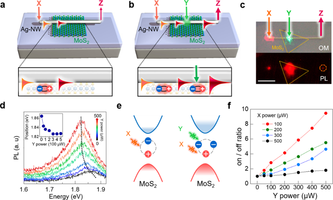
Nanophotonic devices manipulating light for high-speed computing are a counterpart of speed-limited electronic circuits. Although plasmonic circuits are a promising platform for subwavelength miniaturization, the logic-operation principle is still limited to mimicking those of photonic waveguides using phase shifts, polarization, interference, and resonance. Meanwhile, reconfigurable interconversion between exciton and plasmon engender emerging applications like exciton transistors and multiplexers, exciton amplifiers, chiral valleytronics, and nonlinear excitonics. Here, we propose optical logic principles realized by exciton-plasmon interconversion in Ag-nanowires (NW) overlapped on transition metal dichalcogenides (TMDs) monolayers. Excitons generated from TMDs couple to the Ag-NW plasmons, eventually collected as output signals at the Ag-NW end. Using two lasers, we demonstrate AND gate by modulating single excitons in Ag-NW on MoS2 and a half-adder by modulating dual excitons in lateral WSe2 and WS2. Moreover, a 4-to-2 binary encoder is realized in partially overlapped MoSe2 and MoS2 using four-terminal laser inputs. Our results represent great advances in communication processing for optical photonics integrable with subwavelength architectures.
中文翻译:
在2D半导体中通过等离激子-激子互转换进行光学逻辑操作。
操纵光以进行高速计算的纳米光子设备是限速电子电路的对应产品。尽管等离激元电路是实现亚波长小型化的有前途的平台,但逻辑操作原理仍仅限于使用相移,偏振,干扰和谐振来模仿光子波导的逻辑。同时,激子和等离激元之间的可重构互转换引起了诸如激子晶体管和多路复用器,激子放大器,手性山谷电子学和非线性激子电子学等新兴应用。在这里,我们提出了光学逻辑原理,该原理是通过在过渡金属二卤化物(TMDs)单层上重叠的Ag-纳米线(NW)中进行激子-等离子体激元互变而实现的。由TMD产生的激子与Ag-NW等离子体激元耦合,最终在Ag-NW端收集为输出信号。我们使用两个激光,通过在MoS上调制Ag-NW中的单个激子来演示AND门2,并通过在横向WSE调制双重线态激子的半加法器2和WS 2。此外,使用四端激光输入在部分重叠的MoSe 2和MoS 2中实现4到2二进制编码器。我们的结果代表了与亚波长架构集成的光子学通信处理的巨大进步。


 京公网安备 11010802027423号