Microsystems & Nanoengineering ( IF 7.3 ) Pub Date : 2019-04-22 , DOI: 10.1038/s41378-019-0052-7 B X E Desbiolles 1 , A Bertsch 1 , P Renaud 1
|
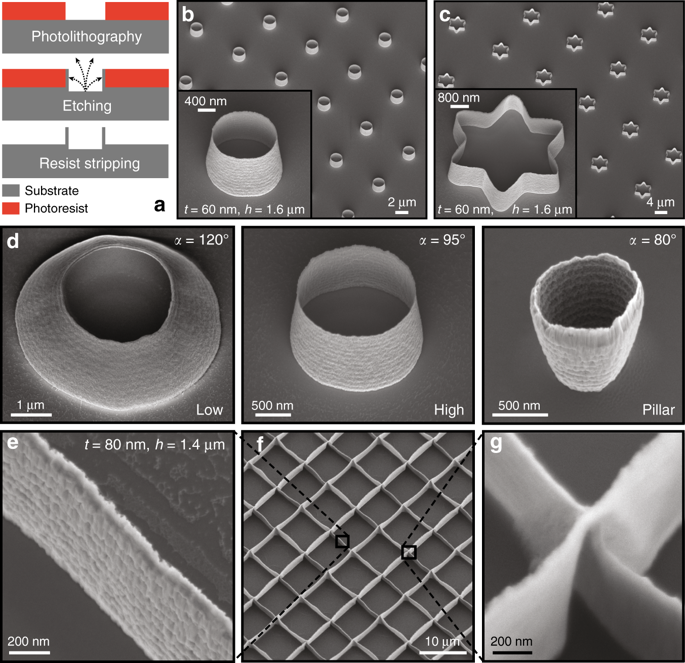
A novel fabrication method based on the local sputtering of photoresist sidewalls during ion beam etching is presented. This method allows for the manufacture of three-dimensional multimaterial nanostructures at the wafer scale in only four process steps. Features of various shapes and profiles can be fabricated at sub-100-nm dimensions with unprecedented freedom in material choice. Complex nanostructures such as nanochannels, multimaterial nanowalls, and suspended networks were successfully fabricated using only standard microprocessing tools. This provides an alternative to traditional nanofabrication techniques, as well as new opportunities for biosensing, nanofluidics, nanophotonics, and nanoelectronics.
中文翻译:
用于 3D 多材料纳米结构制造的离子束蚀刻再沉积
提出了一种基于离子束蚀刻期间光刻胶侧壁局部溅射的新型制造方法。该方法只需四个工艺步骤即可在晶圆级制造三维多材料纳米结构。各种形状和轮廓的特征可以在亚 100 纳米尺寸下制造,并且材料选择具有前所未有的自由度。仅使用标准微处理工具即可成功制造复杂的纳米结构,例如纳米通道、多材料纳米墙和悬浮网络。这为传统纳米制造技术提供了替代方案,也为生物传感、纳米流体、纳米光子学和纳米电子学提供了新的机遇。


 京公网安备 11010802027423号