当前位置:
X-MOL 学术
›
Opt. Lett.
›
论文详情
Our official English website, www.x-mol.net, welcomes your feedback! (Note: you will need to create a separate account there.)
Development of an X-ray imaging detector to resolve 200 nm line-and-space patterns by using transparent ceramics layers bonded by solid-state diffusion
Optics Letters ( IF 3.1 ) Pub Date : 2019-03-12 , DOI: 10.1364/ol.44.001403 Takashi Kameshima , Akihisa Takeuchi , Kentaro Uesugi , Togo Kudo , Yoshiki Kohmura , Kenji Tamasaku , Katsuhiro Muramatsu , Takagimi Yanagitani , Makina Yabashi , Takaki Hatsui
Optics Letters ( IF 3.1 ) Pub Date : 2019-03-12 , DOI: 10.1364/ol.44.001403 Takashi Kameshima , Akihisa Takeuchi , Kentaro Uesugi , Togo Kudo , Yoshiki Kohmura , Kenji Tamasaku , Katsuhiro Muramatsu , Takagimi Yanagitani , Makina Yabashi , Takaki Hatsui
|
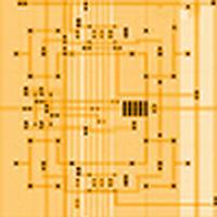
A high-resolution lens-coupled X-ray imaging detector equipped with a thin-layer transparent ceramics scintillator has been developed. The scintillator consists of a 5 μm thick Ce-doped layer (LuAG:Ce) bonded onto the support substrate of the non-doped LuAG ceramics by using a solid-state diffusion technique. Secondary electron microscopy of the bonded interface indicated that the crystal grains were densely packed without any pores in the optical wavelength scale, indicating a quasi-uniform refractive index across the interface. This guarantees high transparency and minimum reflection, which are essential properties for X-ray imaging detectors. The LuAG:Ce scintillator was incorporated into an X-ray imaging detector coupled with an objective lens with a numerical aperture of 0.85 and an optical magnification of 100. The scintillation light was imaged onto a complementary metal–oxide–semiconductor image sensor. The effective pixel size on the scintillator plane was 65 nm. X-ray transmission images of 200 nm line-and-space patterns were successfully resolved. The high spatial resolution was demonstrated by X-ray transmission images of large integrated circuits with the wiring patterns clearly visualized.
中文翻译:

开发X射线成像检测器,以通过使用通过固态扩散结合的透明陶瓷层来分辨200 nm的线和空间图案
已经开发了配备有薄层透明陶瓷闪烁体的高分辨率透镜耦合X射线成像检测器。闪烁体由5μm厚的Ce掺杂组成通过使用固态扩散技术将层(LuAG:Ce)粘结到非掺杂LuAG陶瓷的支撑衬底上。结合界面的二次电子显微镜表明,晶粒紧密堆积,在光波长范围内没有任何孔,表明在界面上的准均匀折射率。这保证了高透明度和最小反射率,这是X射线成像检测器的基本特性。LuAG:Ce闪烁体被结合到X射线成像检测器中,该检测器与物镜的数值孔径为0.85,光学放大倍数为100。闪烁光被成像到互补的金属-氧化物-半导体图像传感器上。闪烁体平面上的有效像素大小为65 nm。成功解析了200 nm线和间隔图案的X射线透射图像。大型集成电路的X射线透射图像显示了高空间分辨率,且布线图清晰可见。
更新日期:2019-03-15
中文翻译:
开发X射线成像检测器,以通过使用通过固态扩散结合的透明陶瓷层来分辨200 nm的线和空间图案
已经开发了配备有薄层透明陶瓷闪烁体的高分辨率透镜耦合X射线成像检测器。闪烁体由5μm厚的Ce掺杂组成通过使用固态扩散技术将层(LuAG:Ce)粘结到非掺杂LuAG陶瓷的支撑衬底上。结合界面的二次电子显微镜表明,晶粒紧密堆积,在光波长范围内没有任何孔,表明在界面上的准均匀折射率。这保证了高透明度和最小反射率,这是X射线成像检测器的基本特性。LuAG:Ce闪烁体被结合到X射线成像检测器中,该检测器与物镜的数值孔径为0.85,光学放大倍数为100。闪烁光被成像到互补的金属-氧化物-半导体图像传感器上。闪烁体平面上的有效像素大小为65 nm。成功解析了200 nm线和间隔图案的X射线透射图像。大型集成电路的X射线透射图像显示了高空间分辨率,且布线图清晰可见。


 京公网安备 11010802027423号