Our official English website, www.x-mol.net, welcomes your
feedback! (Note: you will need to create a separate account there.)
Defect-Controlled Nucleation and Orientation of WSe2 on hBN: A Route to Single-Crystal Epitaxial Monolayers
ACS Nano ( IF 15.8 ) Pub Date : 2019-02-13 00:00:00 , DOI: 10.1021/acsnano.8b09230
Xiaotian Zhang , Fu Zhang , Yuanxi Wang , Daniel S. Schulman , Tianyi Zhang , Anushka Bansal , Nasim Alem , Saptarshi Das , Vincent H. Crespi , Mauricio Terrones , Joan M. Redwing
ACS Nano ( IF 15.8 ) Pub Date : 2019-02-13 00:00:00 , DOI: 10.1021/acsnano.8b09230
Xiaotian Zhang , Fu Zhang , Yuanxi Wang , Daniel S. Schulman , Tianyi Zhang , Anushka Bansal , Nasim Alem , Saptarshi Das , Vincent H. Crespi , Mauricio Terrones , Joan M. Redwing
|
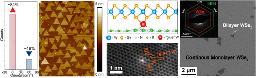
A defect-controlled approach for the nucleation and epitaxial growth of WSe2 on hBN is demonstrated. The WSe2 domains exhibit a preferred orientation of over 95%, leading to a reduced density of inversion domain boundaries (IDBs) upon coalescence. First-principles calculations and experimental studies as a function of growth conditions and substrate pretreatment confirm that WSe2 nucleation density and orientation are controlled by the hBN surface defect density rather than thermodynamic factors. Detailed transmission electron microscopy analysis provides support for the role of single-atom vacancies on the hBN surface that trap W atoms and break surface symmetry leading to a reduced formation energy for one orientation of WSe2 domains. Through careful control of nucleation and extended lateral growth time, fully coalesced WSe2 monolayer films on hBN were achieved. Low-temperature photoluminescence (PL) measurements and transport measurements of back-gated field-effect transistor devices fabricated on WSe2/hBN films show improved optical and electrical properties compared to films grown on sapphire under similar conditions. Our results reveal an important nucleation mechanism for the epitaxial growth of van der Waals heterostructures and demonstrate hBN as a superior substrate for single-crystal transition-metal dichalcogenide (TMD) films, resulting in a reduced density of IDBs and improved properties. The results motivate further efforts focused on the development of single crystal hBN substrates and epilayers for synthesis of wafer-scale single crystal TMD films.
中文翻译:

hBN上WSe 2的缺陷控制形核和取向:通往单晶外延单层的途径。
证明了一种缺陷控制的方法,用于在hBN上形成WSe 2的成核和外延生长。WSe 2结构域显示出超过95%的优选方向,导致合并时反转域边界(IDB)的密度降低。作为生长条件和底物预处理的函数的第一性原理计算和实验研究证实,WSe 2的成核密度和取向是由hBN表面缺陷密度而不是热力学因素控制的。详细的透射电子显微镜分析为hBN表面单原子空位的作用提供了支持,该空位捕获W原子并破坏表面对称性,导致WSe 2某一方向的形成能降低。域。通过仔细控制成核作用和延长横向生长时间,在hBN上获得了完全融合的WSe 2单层膜。在WSe 2上制造的背栅场效应晶体管器件的低温光致发光(PL)测量和传输测量与在相似条件下在蓝宝石上生长的薄膜相比,/ hBN薄膜显示出改进的光学和电学性能。我们的结果揭示了范德华异质结构外延生长的重要成核机理,并证明了hBN作为单晶过渡金属二硫代双氰胺(TMD)膜的优越基底,从而导致IDB密度降低和性能提高。该结果激发了进一步的努力,致力于开发用于晶圆级单晶TMD膜的合成的单晶hBN衬底和外延层。
更新日期:2019-02-13
中文翻译:
hBN上WSe 2的缺陷控制形核和取向:通往单晶外延单层的途径。
证明了一种缺陷控制的方法,用于在hBN上形成WSe 2的成核和外延生长。WSe 2结构域显示出超过95%的优选方向,导致合并时反转域边界(IDB)的密度降低。作为生长条件和底物预处理的函数的第一性原理计算和实验研究证实,WSe 2的成核密度和取向是由hBN表面缺陷密度而不是热力学因素控制的。详细的透射电子显微镜分析为hBN表面单原子空位的作用提供了支持,该空位捕获W原子并破坏表面对称性,导致WSe 2某一方向的形成能降低。域。通过仔细控制成核作用和延长横向生长时间,在hBN上获得了完全融合的WSe 2单层膜。在WSe 2上制造的背栅场效应晶体管器件的低温光致发光(PL)测量和传输测量与在相似条件下在蓝宝石上生长的薄膜相比,/ hBN薄膜显示出改进的光学和电学性能。我们的结果揭示了范德华异质结构外延生长的重要成核机理,并证明了hBN作为单晶过渡金属二硫代双氰胺(TMD)膜的优越基底,从而导致IDB密度降低和性能提高。该结果激发了进一步的努力,致力于开发用于晶圆级单晶TMD膜的合成的单晶hBN衬底和外延层。


 京公网安备 11010802027423号