Our official English website, www.x-mol.net, welcomes your
feedback! (Note: you will need to create a separate account there.)
Asymmetrically Encapsulated Vertical ITO/MoS2/Cu2O Photodetector with Ultrahigh Sensitivity
Small ( IF 13.0 ) Pub Date : 2017-11-24 , DOI: 10.1002/smll.201702066
Sangeeth Kallatt 1, 2 , Smitha Nair 2 , Kausik Majumdar 1
Small ( IF 13.0 ) Pub Date : 2017-11-24 , DOI: 10.1002/smll.201702066
Sangeeth Kallatt 1, 2 , Smitha Nair 2 , Kausik Majumdar 1
Affiliation
|
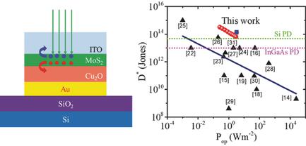
Strong light absorption, coupled with moderate carrier transport properties, makes 2D layered transition metal dichalcogenide semiconductors promising candidates for low intensity photodetection applications. However, the performance of these devices is severely bottlenecked by slow response with persistent photocurrent due to long lived charge trapping, and nonreliable characteristics due to undesirable ambience and substrate effects. Here ultrahigh specific detectivity (D*) of 3.2 × 10¹⁴ Jones and responsivity (R) of 5.77 × 10⁴ A W−1 are demonstrated at an optical power density (Pop) of 0.26 W m−2 and external bias (Vext) of −0.5 V in an indium tin oxide/MoS2/copper oxide/Au vertical multi‐heterojunction photodetector exhibiting small carrier transit time. The active MoS2 layer being encapsulated by carrier collection layers allows us to achieve repeatable characteristics over large number of cycles with negligible trap assisted persistent photocurrent. A large D* > 1014 Jones at zero external bias is also achieved due to the built‐in field of the asymmetric photodetector. Benchmarking the performance against existing reports in literature shows a viable pathway for achieving reliable and highly sensitive photodetectors for ultralow intensity photodetection applications.
中文翻译:

具有超高灵敏度的非对称封装垂直ITO / MoS2 / Cu2O光电探测器
强大的光吸收能力以及适度的载流子传输特性使2D层状过渡金属二卤化二硫半导体有望成为低强度光电检测应用的候选材料。但是,由于寿命长的电荷俘获导致持久光电流的缓慢响应,以及由于不良的环境和基板效应而导致的特性不可靠,这些器件的性能严重受到瓶颈的困扰。在光功率密度(P op)为0.26 W m -2且外部偏置为(V)的情况下,显示出3.2×10 14 Jones的超高比探测度(D *)和5.77×10 4 AW -1的响应度(R)。氧化铟锡/ MoS 2 /氧化铜/ Au垂直多异质结光电探测器中的−0.5 V ext)表现出较小的载流子传输时间。载流子收集层封装的有源MoS 2层使我们能够在可忽略的陷阱辅助持久光电流的情况下,在大量循环中实现可重复的特性。由于非对称光电探测器的内置磁场,在零外部偏置条件下也可获得较大的D *> 10 14 Jones。根据文献中的现有报告对性能进行基准测试,表明了为超低强度光电检测应用实现可靠且高度灵敏的光电检测器的可行途径。
更新日期:2017-11-24
中文翻译:
具有超高灵敏度的非对称封装垂直ITO / MoS2 / Cu2O光电探测器
强大的光吸收能力以及适度的载流子传输特性使2D层状过渡金属二卤化二硫半导体有望成为低强度光电检测应用的候选材料。但是,由于寿命长的电荷俘获导致持久光电流的缓慢响应,以及由于不良的环境和基板效应而导致的特性不可靠,这些器件的性能严重受到瓶颈的困扰。在光功率密度(P op)为0.26 W m -2且外部偏置为(V)的情况下,显示出3.2×10 14 Jones的超高比探测度(D *)和5.77×10 4 AW -1的响应度(R)。氧化铟锡/ MoS 2 /氧化铜/ Au垂直多异质结光电探测器中的−0.5 V ext)表现出较小的载流子传输时间。载流子收集层封装的有源MoS 2层使我们能够在可忽略的陷阱辅助持久光电流的情况下,在大量循环中实现可重复的特性。由于非对称光电探测器的内置磁场,在零外部偏置条件下也可获得较大的D *> 10 14 Jones。根据文献中的现有报告对性能进行基准测试,表明了为超低强度光电检测应用实现可靠且高度灵敏的光电检测器的可行途径。


 京公网安备 11010802027423号