当前位置:
X-MOL 学术
›
Nano Lett.
›
论文详情
Our official English website, www.x-mol.net, welcomes your
feedback! (Note: you will need to create a separate account there.)
Controlled Synthesis of High-Quality Monolayered α-In2Se3 via Physical Vapor Deposition
Nano Letters ( IF 9.6 ) Pub Date : 2015-09-16 00:00:00 , DOI: 10.1021/acs.nanolett.5b01590
Jiadong Zhou 1 , Qingsheng Zeng 1 , Danhui Lv 2 , Linfeng Sun 3 , Lin Niu 1 , Wei Fu 1 , Fucai Liu 1 , Zexiang Shen 1, 3 , Chuanhong Jin 2 , Zheng Liu 1, 4
Nano Letters ( IF 9.6 ) Pub Date : 2015-09-16 00:00:00 , DOI: 10.1021/acs.nanolett.5b01590
Jiadong Zhou 1 , Qingsheng Zeng 1 , Danhui Lv 2 , Linfeng Sun 3 , Lin Niu 1 , Wei Fu 1 , Fucai Liu 1 , Zexiang Shen 1, 3 , Chuanhong Jin 2 , Zheng Liu 1, 4
Affiliation
|
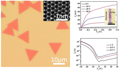
In this work, we have demonstrated the synthesis of high-quality monolayered α-In2Se3 using physical vapor deposition method under atmospheric pressure. The quality of the In2Se3 atomic layers has been confirmed by complementary characterization technologies such as Raman/photoluminescence spectroscopies and atomic force microscope. The atomically resolved images have been obtained by the annular dark-field scanning transmission electron microscope. The field-effect transistors have been fabricated using the atomically layered In2Se3 and exhibit p-type semiconducting behaviors with the mobility up to 2.5 cm2/ Vs. The In2Se3 layers also show a good photoresponsivity of 340A/W, as well as 6 ms response time for the rise and 12 ms for the fall. These results make In2Se3 atomic layers a promising candidate for the optoelectronic and photosensitive device applications.
中文翻译:

高品质的单层控制合成α-在2硒3经由物理气相沉积
在这项工作中,我们已经证明的高品质的合成单层α-在2硒3使用在大气压下的物理气相沉积法。In 2 Se 3原子层的质量已通过互补的表征技术(如拉曼/光致发光光谱法和原子力显微镜)得到证实。通过环形暗场扫描透射电子显微镜已经获得了原子分辨的图像。场效应晶体管是使用原子层状的In 2 Se 3制成的,具有p型半导体行为,迁移率高达2.5 cm 2 / Vs。In 2 Se3层也显示出340A / W的良好光响应性,上升的响应时间为6 ms,下降的响应时间为12 ms。这些结果使In 2 Se 3原子层成为光电子和光敏器件应用的有希望的候选者。
更新日期:2015-09-16
中文翻译:
高品质的单层控制合成α-在2硒3经由物理气相沉积
在这项工作中,我们已经证明的高品质的合成单层α-在2硒3使用在大气压下的物理气相沉积法。In 2 Se 3原子层的质量已通过互补的表征技术(如拉曼/光致发光光谱法和原子力显微镜)得到证实。通过环形暗场扫描透射电子显微镜已经获得了原子分辨的图像。场效应晶体管是使用原子层状的In 2 Se 3制成的,具有p型半导体行为,迁移率高达2.5 cm 2 / Vs。In 2 Se3层也显示出340A / W的良好光响应性,上升的响应时间为6 ms,下降的响应时间为12 ms。这些结果使In 2 Se 3原子层成为光电子和光敏器件应用的有希望的候选者。


 京公网安备 11010802027423号