Nano Energy ( IF 16.8 ) Pub Date : 2017-10-06 , DOI: 10.1016/j.nanoen.2017.10.016 Dmitry Mikulik , Maria Ricci , Gozde Tutuncuoglu , Federico Matteini , Jelena Vukajlovic , Natasa Vulic , Esther Alarcon-Llado , Anna Fontcuberta i Morral
|
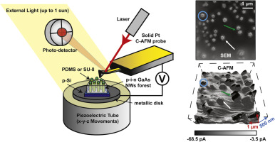
The photonic properties of nanowires advocate for their utilization in next generation solar cells. Compared to traditional devices, the electric scheme is transformed from a single into an ensemble of pn junctions connected in parallel. This new configuration requires new schemes for the characterization. We show how conductive-probe atomic force microscopy, C-AFM, is an essential tool for the characterization and optimization of this parallel-connected nanowire devices. With C-AFM it is possible to obtain both surface topography and local electrical characterization with nanoscale resolution. We demonstrate topography and current mapping of nanowire forests, combined with current-voltage measurements of the individual nanowire junctions from the ensemble. Our results provide discussion elements on some factors limiting the performance of a nanowire-based solar cell and thereby to provide a path for their improvement.
中文翻译:

导电探针原子力显微镜作为基于纳米线的太阳能电池的表征工具
纳米线的光子特性主张将其用于下一代太阳能电池。与传统设备相比,电方案已从单个转换为并联连接的pn结的集合。此新配置需要用于表征的新方案。我们展示了导电探针原子力显微镜C-AFM是如何表征和优化此并联纳米线器件的重要工具。使用C-AFM,可以获得纳米级分辨率的表面形貌和局部电学特征。我们展示了纳米线森林的地形和电流图,并结合了来自集合体的各个纳米线结的电流-电压测量结果。










 京公网安备 11010802027423号