Our official English website, www.x-mol.net, welcomes your
feedback! (Note: you will need to create a separate account there.)
Low-Temperature Growth of Hydrogenated Amorphous Silicon Carbide Solar Cell by Inductively Coupled Plasma Deposition Toward High Conversion Efficiency in Indoor Lighting.
Scientific Reports ( IF 3.8 ) Pub Date : 2017-Oct-05 , DOI: 10.1038/s41598-017-10661-y Ming-Hsuan Kao , Chang-Hong Shen , Pei-chen Yu , Wen-Hsien Huang , Yu-Lun Chueh , Jia-Min Shieh
Scientific Reports ( IF 3.8 ) Pub Date : 2017-Oct-05 , DOI: 10.1038/s41598-017-10661-y Ming-Hsuan Kao , Chang-Hong Shen , Pei-chen Yu , Wen-Hsien Huang , Yu-Lun Chueh , Jia-Min Shieh
|
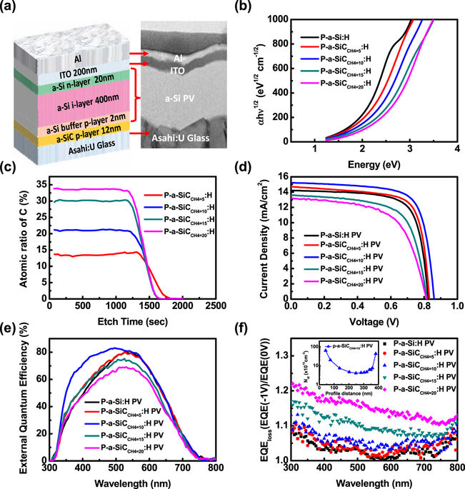
A p-a-SiC:H window layer was used in amorphous Si thin film solar cells to boost the conversion efficiency in an indoor lighting of 500 lx. The p-a-SiC:H window layer/p-a-Si:H buffer layer scheme moderates the abrupt band bending across the p/i interface for the enhancement of VOC, JSC and FF in the solar spectra of short wavelengths. The optimized thickness of i-a-Si:H absorber layer is 400 nm to achieve the conversion efficiency of ~9.58% in an AM1.5 G solar spectrum. However, the optimized thickness of the absorber layer can be changed from 400 to 600 nm in the indoor lighting of 500 lx, exhibiting the maximum output power of 25.56 μW/cm2. Furthermore, various durability tests with excellent performance were investigated, which are significantly beneficial to harvest the indoor lights for applications in the self-powered internet of thing (IoT).
中文翻译:

电感耦合等离子体沉积在室内照明中实现高转换效率的低温生长氢化非晶碳化硅太阳能电池。
在非晶硅薄膜太阳能电池中使用了pa-SiC:H窗口层,以提高500 lx室内照明的转换效率。pa-SiC:H窗口层/ pa-Si:H缓冲层方案可缓和p / i界面上的突变带弯曲,以增强短波长太阳光谱中的V OC,J SC和FF。ia-Si:H吸收层的最优化厚度为400 nm,以在AM1.5 G太阳光谱中实现〜9.58%的转换效率。但是,在500 lx的室内照明条件下,吸收层的最佳厚度可以从400 nm更改为600 nm,最大输出功率为25.56μW/ cm 2。。此外,还对各种性能优异的耐用性测试进行了研究,这些测试对于为自动供电的物联网(IoT)中的应用收集室内照明灯非常有利。
更新日期:2017-10-05
中文翻译:
电感耦合等离子体沉积在室内照明中实现高转换效率的低温生长氢化非晶碳化硅太阳能电池。
在非晶硅薄膜太阳能电池中使用了pa-SiC:H窗口层,以提高500 lx室内照明的转换效率。pa-SiC:H窗口层/ pa-Si:H缓冲层方案可缓和p / i界面上的突变带弯曲,以增强短波长太阳光谱中的V OC,J SC和FF。ia-Si:H吸收层的最优化厚度为400 nm,以在AM1.5 G太阳光谱中实现〜9.58%的转换效率。但是,在500 lx的室内照明条件下,吸收层的最佳厚度可以从400 nm更改为600 nm,最大输出功率为25.56μW/ cm 2。。此外,还对各种性能优异的耐用性测试进行了研究,这些测试对于为自动供电的物联网(IoT)中的应用收集室内照明灯非常有利。


 京公网安备 11010802027423号