当前位置:
X-MOL 学术
›
Adv. Mater.
›
论文详情
Our official English website, www.x-mol.net, welcomes your
feedback! (Note: you will need to create a separate account there.)
Electrically Driven Reversible Phase Changes in Layered In2Se3 Crystalline Film
Advanced Materials ( IF 27.4 ) Pub Date : 2017-10-04 , DOI: 10.1002/adma.201703568
Min Sup Choi 1, 2 , Byung-ki Cheong 3 , Chang Ho Ra 1 , Suyoun Lee 3 , Jee-Hwan Bae 4 , Sungwoo Lee 5 , Gun-Do Lee 5 , Cheol-Woong Yang 4 , James Hone 2 , Won Jong Yoo 1
Advanced Materials ( IF 27.4 ) Pub Date : 2017-10-04 , DOI: 10.1002/adma.201703568
Min Sup Choi 1, 2 , Byung-ki Cheong 3 , Chang Ho Ra 1 , Suyoun Lee 3 , Jee-Hwan Bae 4 , Sungwoo Lee 5 , Gun-Do Lee 5 , Cheol-Woong Yang 4 , James Hone 2 , Won Jong Yoo 1
Affiliation
|
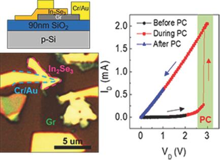
An unconventional phase‐change memory (PCM) made of In2Se3, which utilizes reversible phase changes between a low‐resistance crystalline β phase and a high‐resistance crystalline γ phase is reported for the first time. Using a PCM with a layered crystalline film exfoliated from In2Se3 crystals on a graphene bottom electrode, it is shown that SET/RESET programmed states form via the formation/annihilation of periodic van der Waals' (vdW) gaps (i.e., virtual vacancy layers) in the stack of atomic layers and the concurrent reconfiguration of In and Se atoms across the layers. From density functional theory calculations, β and γ phases, characterized by octahedral bonding with vdW gaps and tetrahedral bonding without vdW gaps, respectively, are shown to have energy bandgap value of 0.78 and 1.86 eV, consistent with a metal‐to‐insulator transition accompanying the β‐to‐γ phase change. The monolithic In2Se3 layered film reported here provides a novel means to achieving a PCM based on melting‐free, low‐entropy phase changes in contrast with the GeTe–Sb2Te3 superlattice film adopted in interfacial phase‐change memory.
中文翻译:

分层In2Se3晶体薄膜中的电驱动可逆相变
首次报道了由In 2 Se 3制成的非常规相变存储器(PCM),该相变存储器利用了低电阻晶体β相和高电阻晶体γ相之间的可逆相变。将PCM与从In 2 Se 3剥落的分层结晶膜一起使用石墨烯底部电极上的晶体,表明SET / RESET编程状态是通过原子层堆叠中周期性范德华(vdW)间隙(即虚拟空位层)的形成/ an灭形成的,并且同时进行了分子的重配置In和Se原子穿过层。根据密度泛函理论计算,分别以具有vdW间隙的八面体键合和无vdW间隙的四面体键合为特征的β和γ相的能带隙值为0.78和1.86 eV,与伴随的金属-绝缘体转变相一致β到γ相变。与GeTe–Sb 2相比,本文报道的单块In 2 Se 3层状膜提供了一种基于无熔融,低熵相变实现PCM的新颖方法界面相变记忆体采用Te 3超晶格薄膜。
更新日期:2017-10-04
中文翻译:
分层In2Se3晶体薄膜中的电驱动可逆相变
首次报道了由In 2 Se 3制成的非常规相变存储器(PCM),该相变存储器利用了低电阻晶体β相和高电阻晶体γ相之间的可逆相变。将PCM与从In 2 Se 3剥落的分层结晶膜一起使用石墨烯底部电极上的晶体,表明SET / RESET编程状态是通过原子层堆叠中周期性范德华(vdW)间隙(即虚拟空位层)的形成/ an灭形成的,并且同时进行了分子的重配置In和Se原子穿过层。根据密度泛函理论计算,分别以具有vdW间隙的八面体键合和无vdW间隙的四面体键合为特征的β和γ相的能带隙值为0.78和1.86 eV,与伴随的金属-绝缘体转变相一致β到γ相变。与GeTe–Sb 2相比,本文报道的单块In 2 Se 3层状膜提供了一种基于无熔融,低熵相变实现PCM的新颖方法界面相变记忆体采用Te 3超晶格薄膜。


 京公网安备 11010802027423号