Nano Research ( IF 9.5 ) Pub Date : 2015-08-27 , DOI: 10.1007/s12274-015-0833-8 Xiang Yuan , Lei Tang , Peng Wang , Zhigang Chen , Yichao Zou , Xiaofeng Su , Cheng Zhang , Yanwen Liu , Weiyi Wang , Cong Liu , Fansheng Chen , Jin Zou , Peng Zhou , Weida Hu , Faxian Xiu
|
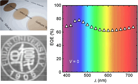
Two-dimensional (2D) materials have attracted substantial attention in electronic and optoelectronic applications with the superior advantages of being flexible, transparent, and highly tunable. Gapless graphene exhibits ultra-broadband and fast photoresponse while the 2D semiconducting MoS2 and GaTe exhibit high sensitivity and tunable responsivity to visible light. However, the device yield and repeatability call for further improvement to achieve large-scale uniformity. Here, we report a layer-by-layer growth of wafer-scale GaTe with a high hole mobility of 28.4 cm2/(V·s) by molecular beam epitaxy. The arrayed p-n junctions were developed by growing few-layer GaTe directly on three-inch Si wafers. The resultant diodes reveal good rectifying characteristics and a high photovoltaic external quantum efficiency up to 62% at 4.8 µW under zero bias. The photocurrent reaches saturation fast enough to capture a time constant of 22 µs and shows no sign of device degradation after 1.37 million cycles of operation. Most strikingly, such high performance has been achieved across the entire wafer, making the volume production of devices accessible. Finally, several photoimages were acquired by the GaTe/Si photodiodes with reasonable contrast and spatial resolution, demonstrating the potential of integrating the 2D materials with silicon technology for novel optoelectronic devices.

中文翻译:
基于几层外延GaTe的晶圆级排列pn结
二维(2D)材料以其柔韧性,透明性和高度可调性的优越性而在电子和光电应用中引起了广泛关注。无间隙石墨烯表现出超宽带和快速的光响应,而二维半导体MoS 2和GaTe表现出对可见光的高灵敏度和可调响应性。但是,器件的成品率和可重复性要求进一步提高以实现大规模的均匀性。在这里,我们报告了具有28.4 cm 2的高空穴迁移率的晶圆级GaTe的逐层生长/(V·s)通过分子束外延。通过在三英寸的Si晶片上直接生长几层GaTe,可以开发出排列的pn结。所得二极管在零偏压下在4.8 µW时具有良好的整流特性和高达62%的高光伏外部量子效率。光电流以足够快的速度达到饱和状态,以捕获22 µs的时间常数,并且在137万次工作循环后没有显示器件性能下降的迹象。最引人注目的是,在整个晶圆上都实现了如此高的性能,从而使设备的批量生产成为可能。最后,GaTe / Si光电二极管以合理的对比度和空间分辨率获得了几张光图像,证明了将2D材料与硅技术集成在一起的潜力,可用于新型光电器件。


 京公网安备 11010802027423号