当前位置:
X-MOL 学术
›
ACS Appl. Mater. Interfaces
›
论文详情
Our official English website, www.x-mol.net, welcomes your
feedback! (Note: you will need to create a separate account there.)
Large Lateral Photovoltage Observed in MoS2 Thickness-Modulated ITO/MoS2/p-Si Heterojunctions
ACS Applied Materials & Interfaces ( IF 8.3 ) Pub Date : 2017-05-11 00:00:00 , DOI: 10.1021/acsami.7b04638
Shuang Qiao 1 , Bin Zhang 1 , Kaiyu Feng 1 , Ridong Cong 1 , Wei Yu 1 , Guangsheng Fu 1 , Shufang Wang 1
ACS Applied Materials & Interfaces ( IF 8.3 ) Pub Date : 2017-05-11 00:00:00 , DOI: 10.1021/acsami.7b04638
Shuang Qiao 1 , Bin Zhang 1 , Kaiyu Feng 1 , Ridong Cong 1 , Wei Yu 1 , Guangsheng Fu 1 , Shufang Wang 1
Affiliation
|
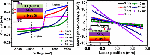
Molybdenum disulfide (MoS2), as a typical two-dimensional (2D) material, has attracted extensive attention in recent years because of its fascinating optical and electric properties. However, the applications of MoS2 have been mainly in photovoltaic devices, field-effect transistors, photodetectors, and gas sensors. Here, it is demonstrated that MoS2 can be found another important application in position sensitive detector (PSD) based on lateral photovoltaic effect (LPE) in it. The ITO/MoS2(3, 5, 7, 9, 10, 20, 50, 100 nm)/p-Si heterojunctions were successfully prepared with vertically standing nanosheet structure of MoS2. Because of the special structure and the strong light absorption of the relatively thick MoS2 film, the ITO/MoS2/p-Si heterojunction exhibits an abnormal thickness-dependent LPE, which can be ascribed to the n- to p-type transformation of MoS2. Moreover, the LPE of ITO/MoS2/p-Si structure improves greatly because of forward enhanced built-in field by type transformation in a wide spectrum response ranging from visible to near-infrared, especially the noticeable improvement in infrared region, indicating its great potential application in infrared PSDs. This work not only suggest that the ITO/MoS2/p-Si heterojunction shows great potential in LPE-based sensors, but also unveils the importance of type transformation of MoS2 in MoS2-based photoelectric devices besides strong light absorption and suitable bandgap.
中文翻译:

在MoS 2厚度调制的ITO / MoS 2 / p-Si异质结中观察到较大的横向光电压
作为典型的二维(2D)材料,二硫化钼(MoS 2)近年来由于其引人入胜的光学和电学性能而引起了广泛的关注。但是,MoS 2的应用主要在光伏设备,场效应晶体管,光电探测器和气体传感器中。在这里,证明了MoS 2可以在基于横向光伏效应(LPE)的位置敏感检测器(PSD)中找到另一个重要应用。使用垂直站立的MoS 2纳米片结构成功制备了ITO / MoS 2(3、5、7、9、10、20、50、100 nm)/ p-Si异质结。由于相对厚的MoS 2膜的特殊结构和强光吸收性,ITO / MoS 2 / p-Si异质结表现出异常的厚度依赖性LPE,这可归因于N-向p型转变。 MoS 2。此外,ITO / MoS 2 / p-Si结构的LPE显着提高,这是因为通过在可见光到近红外范围内的宽光谱响应中的类型转换正向增强了内置场,特别是在红外区域的显着改善,表明了其在红外PSD中具有巨大的潜在应用。这项工作不仅表明ITO / MoS 2/ p-Si异质结在基于LPE的传感器中显示出巨大的潜力,但也揭示了MoS 2的类型转换在基于MoS 2的光电器件中的重要性,除了具有强的光吸收能力和合适的带隙。
更新日期:2017-05-19
中文翻译:
在MoS 2厚度调制的ITO / MoS 2 / p-Si异质结中观察到较大的横向光电压
作为典型的二维(2D)材料,二硫化钼(MoS 2)近年来由于其引人入胜的光学和电学性能而引起了广泛的关注。但是,MoS 2的应用主要在光伏设备,场效应晶体管,光电探测器和气体传感器中。在这里,证明了MoS 2可以在基于横向光伏效应(LPE)的位置敏感检测器(PSD)中找到另一个重要应用。使用垂直站立的MoS 2纳米片结构成功制备了ITO / MoS 2(3、5、7、9、10、20、50、100 nm)/ p-Si异质结。由于相对厚的MoS 2膜的特殊结构和强光吸收性,ITO / MoS 2 / p-Si异质结表现出异常的厚度依赖性LPE,这可归因于N-向p型转变。 MoS 2。此外,ITO / MoS 2 / p-Si结构的LPE显着提高,这是因为通过在可见光到近红外范围内的宽光谱响应中的类型转换正向增强了内置场,特别是在红外区域的显着改善,表明了其在红外PSD中具有巨大的潜在应用。这项工作不仅表明ITO / MoS 2/ p-Si异质结在基于LPE的传感器中显示出巨大的潜力,但也揭示了MoS 2的类型转换在基于MoS 2的光电器件中的重要性,除了具有强的光吸收能力和合适的带隙。


 京公网安备 11010802027423号