当前位置:
X-MOL 学术
›
Appl. Surf. Sci.
›
论文详情
Our official English website, www.x-mol.net, welcomes your
feedback! (Note: you will need to create a separate account there.)
Charged thin film enables dopant free ohmic metal–semiconductor contact formation
Applied Surface Science ( IF 6.3 ) Pub Date : 2025-04-12 , DOI: 10.1016/j.apsusc.2025.163260
Lassi Lahtiluoma, Olli E. Setälä, Ville Vähänissi, Hele Savin
Applied Surface Science ( IF 6.3 ) Pub Date : 2025-04-12 , DOI: 10.1016/j.apsusc.2025.163260
Lassi Lahtiluoma, Olli E. Setälä, Ville Vähänissi, Hele Savin
|
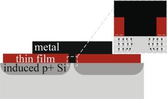
Ohmic contacts are conventionally achieved by externally doping the surface of a semiconductor substrate underneath a metal contact. To avoid the inconveniences that come with heavy doping, we propose an alternative way of achieving an ohmic Al-Si contact utilizing a highly charged atomic layer deposited (ALD) Al2O3 thin film. The idea is to utilize the negative charge of ALD Al2O3 to attract holes towards the surface of the Si substrate and thereby induce a p+ region and consequently an Al/p+ Si contact. The results show that the Al2O3 induced contacts are not only ohmic, but also have a low contact resistivity of 0.24 mΩ⋅cm2. This matches the requirements of various electron devices such as photodiodes indicating potential for the proposed contact formation method.
中文翻译:

带电薄膜可实现无掺杂剂欧姆金属-半导体接触的形成
欧姆触点通常是通过在金属触点下方的半导体衬底表面进行外部掺杂来实现的。为了避免重掺杂带来的不便,我们提出了一种利用高电荷原子层沉积 (ALD) Al 2 O 3 薄膜实现欧姆 Al-Si 接触的替代方法。这个想法是利用 ALD Al 2 O 3 的负电荷将空穴吸引到 Si 衬底表面,从而感应出 p+ 区域,从而产生 Al/p+ Si 接触。结果表明,Al 2 O 3 感应触点不仅是欧姆的,而且具有 0.24 mΩ⋅cm 2 的低接触电阻率。这符合各种电子设备的要求,例如光电二极管,表明所提出的触点形成方法的潜力。
更新日期:2025-04-12
中文翻译:
带电薄膜可实现无掺杂剂欧姆金属-半导体接触的形成
欧姆触点通常是通过在金属触点下方的半导体衬底表面进行外部掺杂来实现的。为了避免重掺杂带来的不便,我们提出了一种利用高电荷原子层沉积 (ALD) Al 2 O 3 薄膜实现欧姆 Al-Si 接触的替代方法。这个想法是利用 ALD Al 2 O 3 的负电荷将空穴吸引到 Si 衬底表面,从而感应出 p+ 区域,从而产生 Al/p+ Si 接触。结果表明,Al 2 O 3 感应触点不仅是欧姆的,而且具有 0.24 mΩ⋅cm 2 的低接触电阻率。这符合各种电子设备的要求,例如光电二极管,表明所提出的触点形成方法的潜力。


 京公网安备 11010802027423号