Light: Science & Applications ( IF 20.6 ) Pub Date : 2025-01-26 , DOI: 10.1038/s41377-025-01751-y
Zhiyuan Liu, Haicheng Cao, Xiao Tang, Tingang Liu, Yi Lu, Zixian Jiang, Na Xiao, Xiaohang Li
|
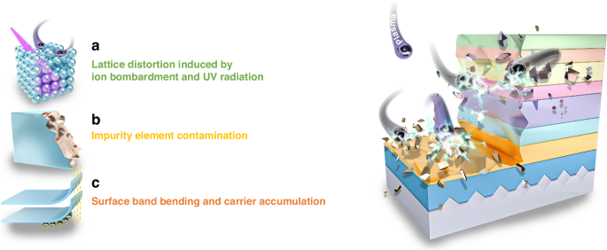
The size of InGaN micro-LEDs is continuously decreasing to meet the demands of various emerging applications, especially in tiny micro-displays such as AR/VR. However, the conventional pixel definition based on plasma etching significantly damages the mesa sidewalls, leading to a severe reduction in efficiency as the micro-LED size decreases. This seriously impedes the development and application of micro-LEDs. In this work, we comprehensively explain the origin of micro-LED sidewall effects and corresponding physical models. Subsequently, we systematically review recent progress in micro-LED fabrication aiming at suppressing sidewall effects. Furthermore, we discuss advancements in micro-LED fabrication with “damage-free” techniques, which hold the potential to fundamentally address the issue of plasma damage in the micro-LED process. We believe this review will deepen the understanding of micro-LED sidewall effects and provide a better insight into the latest associated fabrication technologies for high-efficient InGaN micro-LEDs.
中文翻译:
采用先进 InGaN micro-LED 制造技术,减轻侧壁效应
InGaN micro-LED 的尺寸不断缩小,以满足各种新兴应用的需求,尤其是在 AR/VR 等微型微型显示器中。然而,基于等离子体蚀刻的传统像素定义会严重损坏台面侧壁,导致随着 micro-LED 尺寸的减小,效率严重降低。这严重阻碍了 micro-LED 的发展和应用。在这项工作中,我们全面解释了 micro-LED 侧壁效应的由来和相应的物理模型。随后,我们系统地回顾了旨在抑制侧壁效应的 micro-LED 制造的最新进展。此外,我们还讨论了使用“无损”技术制造 micro-LED 的进步,这些技术有可能从根本上解决 micro-LED 工艺中的等离子体损伤问题。我们相信,本文将加深对 micro-LED 侧壁效应的理解,并更好地了解高效 InGaN micro-LED 的最新相关制造技术。


 京公网安备 11010802027423号