Light: Science & Applications ( IF 20.6 ) Pub Date : 2024-10-09 , DOI: 10.1038/s41377-024-01639-3
Haifeng Wu 1 , Xiao Lin 1, 2 , Qin Shuai 1 , Youliang Zhu 1, 2 , Yi Fu 3 , Xiaoqin Liao 1 , Yazhou Wang 2 , Yizhe Wang 1 , Chaowei Cheng 4 , Yong Liu 1 , Lei Sun 5 , Xinyi Luo 1 , Xiaoli Zhu 1 , Liancheng Wang 4 , Ziwei Li 1 , Xiao Wang 1 , Dong Li 1 , Anlian Pan 1, 6
|
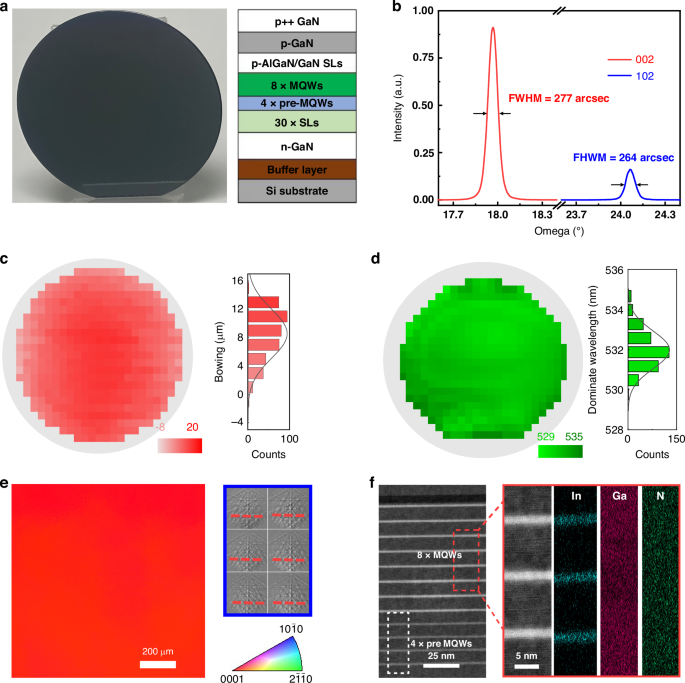
Owing to high pixel density and brightness, gallium nitride (GaN) based micro-light-emitting diodes (Micro-LEDs) are considered revolutionary display technology and have important application prospects in the fields of micro-display and virtual display. However, Micro-LEDs with pixel sizes smaller than 10 μm still encounter technical challenges such as sidewall damage and limited light extraction efficiency, resulting in reduced luminous efficiency and severe brightness non-uniformity. Here, we reported high-brightness green Micro-displays with a 5 μm pixel utilizing high-quality GaN-on-Si epilayers. Four-inch wafer-scale uniform green GaN epilayer is first grown on silicon substrate, which possesses a low dislocation density of 5.25 × 108 cm−2, small wafer bowing of 16.7 μm, and high wavelength uniformity (standard deviation STDEV < 1 nm), scalable to 6-inch sizes. Based on the high-quality GaN epilayers, green Micro-LEDs with 5 μm pixel sizes are designed with vertical non-alignment bonding technology. An atomic sidewall passivation method combined with wet treatment successfully addressed the Micro-LED sidewall damages and steadily produced nano-scale surface textures on the pixel top, which unlocked the internal quantum efficiency of the high-quality green GaN-on-Si epi-wafer. Ultra-high brightness exceeding 107 cd/m2 (nits) is thus achieved in the green Micro-LEDs, marking the highest reported results. Furthermore, integration of Micro-LEDs with Si-based CMOS circuits enables the realization of green Micro-LED displays with resolution up to 1080 × 780, realizing high-definition playback of movies and images. This work lays the foundation for the mass production of high-brightness Micro-LED displays on large-size GaN-on-Si epi-wafers.
中文翻译:
具有晶圆级均匀硅基 GaN 外延层的超高亮度 Micro-LED
由于像素密度和亮度高,基于氮化镓 (GaN) 的微型发光二极管 (Micro-LED) 被认为是革命性的显示技术,在微显示和虚拟显示领域具有重要的应用前景。然而,像素尺寸小于 10 μm 的 Micro-LED 仍面临侧壁损坏和光提取效率受限等技术挑战,导致发光效率降低和严重的亮度不均匀性。在这里,我们报道了利用高质量硅基氮化镓外延层的 5 μm 像素的高亮度绿色微型显示器。四英寸晶圆级均匀绿色 GaN 外延层首先在硅衬底上生长,该衬底具有 5.25 × 108 cm-2 的低位错密度、16.7 μm 的小晶圆弯曲和高波长均匀性(标准偏差 STDEV < 1 nm),可扩展至 6 英寸尺寸。基于高质量的 GaN 外延层,采用垂直非对准键合技术设计了像素尺寸为 5 μm 的绿色 Micro-LED。原子侧壁钝化方法结合湿法处理成功解决了 Micro-LED 侧壁损伤问题,并在像素顶部稳定地产生了纳米级表面纹理,从而释放了高质量绿色硅基氮化镓外延片的内部量子效率。因此,绿色 Micro-LED 实现了超过 107 cd/m2 (nits) 的超高亮度,标志着报告的最高结果。此外,Micro-LED 与硅基 CMOS 电路的集成可实现分辨率高达 1080 × 780 的绿色 Micro-LED 显示器,实现电影和图像的高清播放。 这项工作为在大尺寸硅基氮化镓外延片上大规模生产高亮度 Micro-LED 显示器奠定了基础。


 京公网安备 11010802027423号