当前位置:
X-MOL 学术
›
J. Phys. Chem. Lett.
›
论文详情
Our official English website, www.x-mol.net, welcomes your
feedback! (Note: you will need to create a separate account there.)
Dual-Mode Reconfigurable Split-Gate Logic Transistor through Van der Waals Integration
The Journal of Physical Chemistry Letters ( IF 4.8 ) Pub Date : 2024-09-24 , DOI: 10.1021/acs.jpclett.4c02397 Xue Chen, Haozhe Xue, Yu Wen, Kai You, Bei Jiang, Guanglong Ding, Kui Zhou, Zherui Zhao, Yan Yan, Meng Zhang, Vellaisamy A. L. Roy, Su-Ting Han, Feng Li, Chi-Ching Kuo, Ye Zhou
The Journal of Physical Chemistry Letters ( IF 4.8 ) Pub Date : 2024-09-24 , DOI: 10.1021/acs.jpclett.4c02397 Xue Chen, Haozhe Xue, Yu Wen, Kai You, Bei Jiang, Guanglong Ding, Kui Zhou, Zherui Zhao, Yan Yan, Meng Zhang, Vellaisamy A. L. Roy, Su-Ting Han, Feng Li, Chi-Ching Kuo, Ye Zhou
|
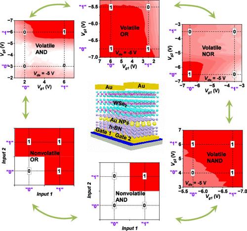
As silicon-based transistors approach their physical size limitations, two-dimensional material-based reconfigurable functional electronic devices are considered the most promising novel device architectures beyond Moore strategies. While these devices have garnered significant attention, they often require complex device fabrication processes and extra electric fields. Additionally, the device performance is usually limited by the metal–semiconductor interface properties. In this Letter, we have constructed a reconfigurable logic device based on a WSe2 transistor with a nanofloating gate and split-gates through van der Waals integration. This device achieves a small Schottky barrier height due to the van der Waals contacts. By varying the split-gate biases, we can realize volatile reconfigurable homojunctions as well as AND, OR, NOR, and NAND logic operations with just a single device. Furthermore, with the charge trapping effect of nanofloating gate, we can also achieve nonvolatile reconfigurable homojunctions, as well as AND and OR logic operations. The volatile and nonvolatile logic operations are similar to the short-term plasticity and long-term plasticity, respectively, of synapses in the human brain. This work offers a potential approach for creating novel reconfigurable functional electronic devices with a simple fabrication process and low cost.
中文翻译:

通过 Van der Waals 集成实现双模可重构分离栅逻辑晶体管
随着硅基晶体管接近其物理尺寸极限,基于二维材料的可重构功能电子器件被认为是超越摩尔策略的最有前途的新型器件架构。虽然这些器件受到了极大的关注,但它们通常需要复杂的器件制造工艺和额外的电场。此外,器件性能通常受到金属-半导体界面特性的限制。在这封信中,我们构建了一个基于 WSe2 晶体管的可重构逻辑器件,该晶体管具有纳米浮动栅极和通过范德华集成实现的分离栅极。由于采用范德华触点,该器件实现了较小的肖特基势垒高度。通过改变分离栅极偏置,我们只需一个器件即可实现易失性可重构同质结以及 AND、OR、NOR 和 NAND 逻辑操作。此外,借助纳米浮栅的电荷捕获效应,我们还可以实现非易失性可重构同质结,以及 AND 和 OR 逻辑操作。volatile 和非 volatile logic 操作分别类似于人脑中突触的短期可塑性和长期可塑性。这项工作为创建具有简单制造工艺和低成本的新型可重构功能电子器件提供了一种潜在的方法。
更新日期:2024-09-24
中文翻译:
通过 Van der Waals 集成实现双模可重构分离栅逻辑晶体管
随着硅基晶体管接近其物理尺寸极限,基于二维材料的可重构功能电子器件被认为是超越摩尔策略的最有前途的新型器件架构。虽然这些器件受到了极大的关注,但它们通常需要复杂的器件制造工艺和额外的电场。此外,器件性能通常受到金属-半导体界面特性的限制。在这封信中,我们构建了一个基于 WSe2 晶体管的可重构逻辑器件,该晶体管具有纳米浮动栅极和通过范德华集成实现的分离栅极。由于采用范德华触点,该器件实现了较小的肖特基势垒高度。通过改变分离栅极偏置,我们只需一个器件即可实现易失性可重构同质结以及 AND、OR、NOR 和 NAND 逻辑操作。此外,借助纳米浮栅的电荷捕获效应,我们还可以实现非易失性可重构同质结,以及 AND 和 OR 逻辑操作。volatile 和非 volatile logic 操作分别类似于人脑中突触的短期可塑性和长期可塑性。这项工作为创建具有简单制造工艺和低成本的新型可重构功能电子器件提供了一种潜在的方法。


 京公网安备 11010802027423号