当前位置:
X-MOL 学术
›
Laser Photonics Rev.
›
论文详情
Our official English website, www.x-mol.net, welcomes your
feedback! (Note: you will need to create a separate account there.)
Multilayer Reconfigurable 3D Photonics Integrated Circuits Based on Deposition Method
Laser & Photonics Reviews ( IF 9.8 ) Pub Date : 2024-09-10 , DOI: 10.1002/lpor.202400827
Xinru Xu 1 , Daming Zhang 1 , Peng Zhang 2 , Bo Tang 2 , Yuexin Yin 1
Laser & Photonics Reviews ( IF 9.8 ) Pub Date : 2024-09-10 , DOI: 10.1002/lpor.202400827
Xinru Xu 1 , Daming Zhang 1 , Peng Zhang 2 , Bo Tang 2 , Yuexin Yin 1
Affiliation
|
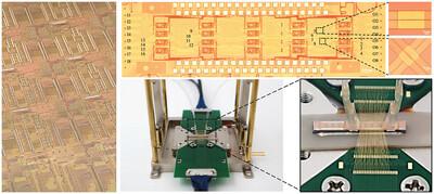
Photonics integrated circuits (PICs) can overcome the bottlenecks in communication capacity. 3D PIC technology is an attractive method for increasing density effectively and combining different materials on one chip for functional integration. In this study, a low-cost and reconfigurable 3D integrated silicon photonics (SiPhs) platform is proposed fabricated by depositing polycrystalline silicon (poly-Si) on crystalline silicon (c-Si), which is patterned through deep ultraviolet (DUV) stepper-based manufacturing process. The high mobility of poly-Si ensures high-speed and power-efficient modulation. Based on the proposed 3D SiPhs platform, an 8 × 8 optical switch whose units are separated in different layers is fabricated and packaged. The switch shows average insertion losses of −13.98 and −15.86 dB, while working in “all-cross” and “all-bar” states, respectively. The crosstalk is lower than −19 and −11 dB for “all-cross” and “all-bar” states. Additionally, an overlayer switch located on the 1st and 3rd layers is proposed and experimentally demonstrated, which offers overlapping capabilities that are more compact compared with switches in a single-layer platform. This validates the possibility of the large-density integration scalability of the platform.
中文翻译:

基于沉积法的多层可重构三维光子集成电路
光子集成电路 (PIC) 可以克服通信容量的瓶颈。3D PIC 技术是一种有吸引力的方法,可以有效提高密度并将不同的材料组合在一个芯片上以实现功能集成。在本研究中,通过在晶体硅 (c-Si) 上沉积多晶硅 (poly-Si) 来制造一种低成本且可重构的 3D 集成硅光子学 (SiPhs) 平台,该平台通过基于深紫外 (DUV) 步进器的制造工艺进行图案化。多晶硅的高迁移率确保了高速和低功耗的调制。基于所提出的 3D SiPhs 平台,制造并封装了一种 8 × 8 光开关,其单元分为不同的层。该开关的平均插入损耗分别为 −13.98 和 −15.86 dB,同时分别在 “all-cross” 和 “all-bar” 状态下工作。对于“all-cross”和“all-bar”状态,串扰低于 −19 和 −11 dB。此外,还提出了一种位于第 1 层和第 3 层的叠加开关,并进行了实验演示,与单层平台中的开关相比,它提供了更紧凑的重叠功能。这验证了该平台的高密度集成可扩展性的可能性。
更新日期:2024-09-10
中文翻译:
基于沉积法的多层可重构三维光子集成电路
光子集成电路 (PIC) 可以克服通信容量的瓶颈。3D PIC 技术是一种有吸引力的方法,可以有效提高密度并将不同的材料组合在一个芯片上以实现功能集成。在本研究中,通过在晶体硅 (c-Si) 上沉积多晶硅 (poly-Si) 来制造一种低成本且可重构的 3D 集成硅光子学 (SiPhs) 平台,该平台通过基于深紫外 (DUV) 步进器的制造工艺进行图案化。多晶硅的高迁移率确保了高速和低功耗的调制。基于所提出的 3D SiPhs 平台,制造并封装了一种 8 × 8 光开关,其单元分为不同的层。该开关的平均插入损耗分别为 −13.98 和 −15.86 dB,同时分别在 “all-cross” 和 “all-bar” 状态下工作。对于“all-cross”和“all-bar”状态,串扰低于 −19 和 −11 dB。此外,还提出了一种位于第 1 层和第 3 层的叠加开关,并进行了实验演示,与单层平台中的开关相比,它提供了更紧凑的重叠功能。这验证了该平台的高密度集成可扩展性的可能性。


 京公网安备 11010802027423号