Nature ( IF 50.5 ) Pub Date : 2024-08-14 , DOI: 10.1038/s41586-024-07785-3 Chi Liu 1, 2 , Xin-Zhe Wang 1, 2 , Cong Shen 3 , Lai-Peng Ma 1, 2 , Xu-Qi Yang 1, 2 , Yue Kong 1, 2 , Wei Ma 1, 2 , Yan Liang 1, 2 , Shun Feng 1, 2 , Xiao-Yue Wang 1, 2 , Yu-Ning Wei 1, 2 , Xi Zhu 1, 2 , Bo Li 1, 2 , Chang-Ze Li 1, 2 , Shi-Chao Dong 1, 2 , Li-Ning Zhang 3 , Wen-Cai Ren 1, 2 , Dong-Ming Sun 1, 2 , Hui-Ming Cheng 1, 2, 4
|
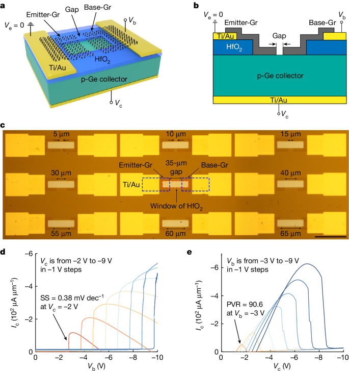
Hot-carrier transistors are a class of devices that leverage the excess kinetic energy of carriers. Unlike regular transistors, which rely on steady-state carrier transport, hot-carrier transistors modulate carriers to high-energy states, resulting in enhanced device speed and functionality. These characteristics are essential for applications that demand rapid switching and high-frequency operations, such as advanced telecommunications and cutting-edge computing technologies1,2,3,4,5. However, the traditional mechanisms of hot-carrier generation are either carrier injection6,7,8,9,10,11 or acceleration12,13, which limit device performance in terms of power consumption and negative differential resistance14,15,16,17. Mixed-dimensional devices, which combine bulk and low-dimensional materials, can offer different mechanisms for hot-carrier generation by leveraging the diverse potential barriers formed by energy-band combinations18,19,20,21. Here we report a hot-emitter transistor based on double mixed-dimensional graphene/germanium Schottky junctions that uses stimulated emission of heated carriers to achieve a subthreshold swing lower than 1 millivolt per decade beyond the Boltzmann limit and a negative differential resistance with a peak-to-valley current ratio greater than 100 at room temperature. Multi-valued logic with a high inverter gain and reconfigurable logic states are further demonstrated. This work reports a multifunctional hot-emitter transistor with significant potential for low-power and negative-differential-resistance applications, marking a promising advancement for the post-Moore era.
中文翻译:
一种基于热载流子受激发射的热发射极晶体管
热载流子晶体管是一类利用载流子多余动能的器件。与依赖稳态载流子传输的常规晶体管不同,热载流子晶体管将载流子调制到高能态,从而提高了器件速度和功能。这些特性对于需要快速切换和高频操作的应用至关重要,例如先进电信和尖端计算技术1,2,3,4,5 。然而,传统的热载流子生成机制要么是载流子注入6,7,8,9,10,11要么是加速12,13 ,这限制了器件在功耗和负微分电阻方面的性能14,15,16, 17 .混合维器件结合了块体和低维材料,可以通过利用能带组合形成的不同势垒来提供不同的热载流子生成机制18,19,20,21 。在这里,我们报告了一种基于双混合维石墨烯/锗肖特基结的热发射极晶体管,该晶体管利用热载流子的受激发射来实现超出玻尔兹曼极限的每十年低于 1 毫伏的亚阈值摆幅以及具有峰值的负微分电阻。室温下谷电流比大于 100。进一步演示了具有高逆变器增益和可重构逻辑状态的多值逻辑。这项工作报告了一种多功能热发射极晶体管,在低功耗和负微分电阻应用方面具有巨大潜力,标志着后摩尔时代的一个有希望的进步。


 京公网安备 11010802027423号