npj Quantum Information ( IF 6.6 ) Pub Date : 2024-08-14 , DOI: 10.1038/s41534-024-00868-z Janka Biznárová , Amr Osman , Emil Rehnman , Lert Chayanun , Christian Križan , Per Malmberg , Marcus Rommel , Christopher Warren , Per Delsing , August Yurgens , Jonas Bylander , Anita Fadavi Roudsari
|
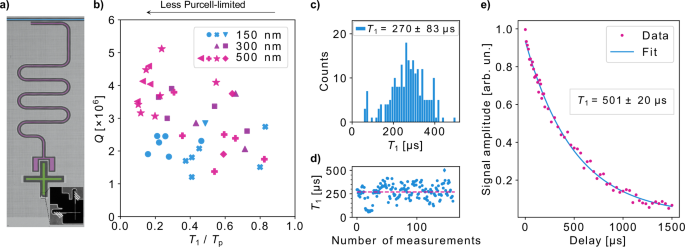
We demonstrate aluminum-on-silicon planar transmon qubits with time-averaged T1 energy relaxation times of up to 270 μs, corresponding to Q = 5 million, and a highest observed value of 501 μs. Through materials analysis techniques and numerical simulations we investigate the dominant source of energy loss, and devise and demonstrate a strategy toward its mitigation. Growing aluminum films thicker than 300 nm reduces the presence of oxide, a known host of defects, near the substrate-metal interface, as confirmed by time-of-flight secondary ion mass spectrometry. A loss analysis of coplanar waveguide resonators shows that this results in a reduction of dielectric loss due to two-level system defects. The correlation between the enhanced performance of our devices and the film thickness is due to the aluminum growth in columnar structures of parallel grain boundaries: transmission electron microscopy shows larger grains in the thicker film, and consequently fewer grain boundaries containing oxide near the substrate-metal interface.
中文翻译:
减轻铝硅超导量子位中的界面介电损耗
我们展示了铝基硅平面传输量子位,其时间平均T 1能量弛豫时间高达 270 μs,相当于Q = 500 万,最高观测值为 501 μs。通过材料分析技术和数值模拟,我们研究了能量损失的主要来源,并设计和论证了缓解策略。飞行时间二次离子质谱法证实,生长厚度超过 300 nm 的铝膜可减少基底-金属界面附近氧化物(一种已知的缺陷)的存在。共面波导谐振器的损耗分析表明,由于两级系统缺陷,这会导致介电损耗降低。我们的器件性能增强与薄膜厚度之间的相关性是由于平行晶界的柱状结构中的铝生长所致:透射电子显微镜显示较厚的薄膜中晶粒较大,因此基底金属附近含有氧化物的晶界较少界面。


 京公网安备 11010802027423号