当前位置:
X-MOL 学术
›
ACS Energy Lett.
›
论文详情
Our official English website, www.x-mol.net, welcomes your
feedback! (Note: you will need to create a separate account there.)
Common Misconceptions in the Analysis of Critical Figures of Merit for Functioning Electrocatalyst/Semiconductor Photoelectrocatalysts under Solar Water-Splitting Conditions
ACS Energy Letters ( IF 19.3 ) Pub Date : 2024-07-29 , DOI: 10.1021/acsenergylett.4c01365 Aarti Mathur 1, 2 , Ahmet Sert 1, 2 , Suljo Linic 1, 2
ACS Energy Letters ( IF 19.3 ) Pub Date : 2024-07-29 , DOI: 10.1021/acsenergylett.4c01365 Aarti Mathur 1, 2 , Ahmet Sert 1, 2 , Suljo Linic 1, 2
Affiliation
|
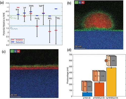
Figure 1. (a) Band edge positions (V vs NHE) at pH = 0 for common SCs used in photoelectrochemical devices. The conduction and valence band positions are shown in the bottom and top bars, respectively, with OER and HER thermodynamic potentials represented as blue and green dashed lines, respectively. The red and blue bars are the oxidation and reduction potentials of each SC. SC will self-oxidize if the oxidation potential is below the OER potential and self-reduce if the reduction potential is above the HER potential. (b, c) STEM cross-sectional images of (b) a Ni nanoparticle electrodeposited on an n-Si wafer, tested under OER reaction conditions, and (c) a planar Ni EC evaporated on an n-Si wafer, tested under OER reaction conditions. (d) Experimental photovoltage plotted for three experimental Ni/n-Si systems. In blue is pf-Ni/n-Si, in orange is pf-Ni/SiO2/n-Si, and in yellow is np-Ni/SiO2/n-Si. Data in panel (a) adapted from ref (13). Remaining data adapted from ref (49). Figure 2. (a) Current density versus voltage (J–V) plots of the illuminated np-Ni/n-Si system over 10–30 cyclic voltammetry sweeps under OER conditions in a base. (b) Nanoparticle size distributions for the np-Ni/n-Si and np-Ni/p+-Si systems shown in panels (a) and (c). (c) Current density versus voltage plots (J–V) of dark np-Ni/p+-Si system over 10–30 cyclic voltammetry sweeps under OER conditions in a base. (d) Photovoltage as a function of cyclic voltammetry sweeps for pf-Ni/n-Si, pf-Ni/SiO2/n-Si, and np-Ni/n-Si, showing that the photovoltage remains nearly constant under the reaction conditions. Data adapted from ref (49). Figure 3. (a) High-resolution TEM cross section of the np-Ni/Si interface. (b) Illustration of the energy band diagram and the movement of charge carriers for a metal EC/insulator/SC interface in equilibrium with relevant physical parameters. Here, Esol is the solution Fermi level, Em is the metal EC Fermi level, Es is the SC Fermi level, ECB is the conduction band energy level, EVB is the valence band energy level, ϕb is the barrier height, ϕe is the potential barrier height for electrons, d is the thickness of the insulator, Vn is the difference between the SC Fermi level and the conduction band edge, Vfb is the flat band potential, Je is the electron current density, and Js is the reverse saturation current density. (c) Measured photovoltage as a function of the insulator thickness for pf-Ir/HfO2/n-Si and pf-Ni/HfO2/n-Si systems, with data adapted from refs (13) and (24). Figure 4. (a) Experimentally derived ideal barrier height and actual barrier height for pf-Ni/n-Si and pf-Ni/SiO2/n-Si systems. (b) Current density versus voltage (J–V) curves of pf-Ni/SiO2/Si systems as well as computational model fits and model error bounds. (c) Current density versus voltage (J–V) curves of np-Ni/Si systems as well as computational model fits and model error bounds. (d) Recombination currents depicted for three systems: pf-Ni/n-Si, pf-Ni/SiO2/n-Si, and np-Ni/n-Si, broken down further into contributions from the barrier height (ϕb), oxide tunneling probability (Tt), and catalyst coverage (fc). Data adapted from ref (49). Figure 5. (a) Energy band diagram describing the “pinch-off” effect, where a metal contact is surrounded by an oxide shell with a high work function, causing the overall system barrier height to increase compared to the metal contact barrier height. Here, Vbb is the degree of band bending and Δ is the difference in the barrier height of the high-barrier and low-barrier contacts. (b) Schematic of COMSOL model setup with a Ni nanoparticle surrounded by a high-barrier shell, in contact with an illuminated semiconductor. (c–e) Simulated conduction band edge potentials (V vs Ef) through the center of the nanoparticle for varying high-barrier shell thicknesses of (c) 15 nm, (d) 30 nm, and (e) 45 nm Ni nanoparticles. A.M. and A.S. contributed equally. The authors acknowledge support from the U.S. Department of Energy, Office of Basic Energy Sciences, Division of Chemical Sciences (DE-SC0021362). This article references 77 other publications. This article has not yet been cited by other publications.
中文翻译:

太阳能水分解条件下功能电催化剂/半导体光电催化剂的关键品质因数分析中的常见误解
图 1. (a) pH = 0 时光电化学器件中使用的常见 SC 的能带边缘位置(V 与 NHE)。导带和价带位置分别显示在底部和顶部条形图中,OER 和 HER 热力学势分别表示为蓝色和绿色虚线。红色和蓝色条是每个 SC 的氧化和还原电位。如果氧化电位低于 OER 电位,SC 将自氧化;如果还原电位高于 HER 电位,SC 将自还原。 (b, c) (b) 在 OER 反应条件下测试的 n-Si 晶圆上电沉积的 Ni 纳米颗粒的 STEM 横截面图像,以及 (c) 在 OER 反应条件下测试的在 n-Si 晶圆上蒸发的平面 Ni EC 的 STEM 横截面图像反应条件。 (d) 绘制了三个实验 Ni/n-Si 系统的实验光电压。蓝色为pf-Ni/n-Si,橙色为pf-Ni/SiO 2 /n-Si,黄色为np-Ni/SiO 2 /n-Si。 (a) 图中的数据改编自参考文献 (13)。其余数据改编自参考文献(49)。图 2. (a) 在 OER 条件下,在基底中进行 10-30 次循环伏安扫描后,照明 np-Ni/n-Si 系统的电流密度与电压 ( J–V ) 图。 (b) np-Ni/n-Si 和 np-Ni/p + -Si 系统的纳米颗粒尺寸分布如图 (a) 和 (c) 所示。 (c) 在 OER 条件下,暗 np-Ni/p + -Si 体系经过 10-30 次循环伏安扫描后的电流密度与电压图 ( J–V )。 (d) pf-Ni/n-Si、pf-Ni/SiO 2 /n-Si 和 np-Ni/n-Si 的光电压作为循环伏安扫描的函数,表明光电压在反应下几乎保持恒定状况。数据改编自参考文献 (49)。图 3. (a) np-Ni/Si 界面的高分辨率 TEM 横截面。 (b) 与相关物理参数处于平衡状态的金属 EC/绝缘体/SC 界面的能带图和载流子运动的图示。其中, E sol为溶液费米能级, E m为金属 EC 费米能级, E s为 SC 费米能级, E CB为导带能级, E VB为价带能级,ψ b为势垒高度, phi e是电子势垒高度, d是绝缘体厚度, V n是 SC 费米能级与导带边缘之间的差值, V fb是平带电势, J e是电子电流密度, J s为反向饱和电流密度。 (c)测量的pf-Ir/HfO 2 /n-Si和pf-Ni/HfO 2 /n-Si系统的光电压与绝缘体厚度的函数关系,数据改编自参考文献(13)和(24)。图 4. (a) 实验得出的 pf-Ni/n-Si 和 pf-Ni/SiO 2 /n-Si 系统的理想势垒高度和实际势垒高度。 (b) pf-Ni/SiO 2 /Si 系统的电流密度与电压 ( J–V ) 曲线以及计算模型拟合和模型误差范围。 (c) np-Ni/Si 系统的电流密度与电压 ( J-V ) 曲线以及计算模型拟合和模型误差范围。 (d) 描述了三个系统的复合电流:pf-Ni/n-Si、pf-Ni/SiO 2 /n-Si 和 np-Ni/n-Si,进一步细分为势垒高度 (ψ b ) 的贡献)、氧化物隧道概率( T t )和催化剂覆盖率( f c )。数据改编自参考文献 (49)。图 5.(a) 描述“夹断”效应的能带图,其中金属接触被具有高功函数的氧化物壳包围,导致整个系统势垒高度与金属接触势垒高度相比增加。这里, V bb是能带弯曲程度,Δ是高势垒和低势垒接触的势垒高度差。 (b) COMSOL 模型设置示意图,其中镍纳米颗粒被高势垒壳包围,并与发光半导体接触。 (c–e) 对于 (c) 15 nm、(d) 30 nm 和 (e) 45 nm Ni 纳米粒子的不同高势垒壳厚度,通过纳米粒子中心的模拟导带边缘电势( V与E f ) 。 AM 和 AS 的贡献相等。作者感谢美国能源部基础能源科学办公室化学科学部 (DE-SC0021362) 的支持。本文引用了 77 篇其他出版物。这篇文章尚未被其他出版物引用。
更新日期:2024-07-29
中文翻译:
太阳能水分解条件下功能电催化剂/半导体光电催化剂的关键品质因数分析中的常见误解
图 1. (a) pH = 0 时光电化学器件中使用的常见 SC 的能带边缘位置(V 与 NHE)。导带和价带位置分别显示在底部和顶部条形图中,OER 和 HER 热力学势分别表示为蓝色和绿色虚线。红色和蓝色条是每个 SC 的氧化和还原电位。如果氧化电位低于 OER 电位,SC 将自氧化;如果还原电位高于 HER 电位,SC 将自还原。 (b, c) (b) 在 OER 反应条件下测试的 n-Si 晶圆上电沉积的 Ni 纳米颗粒的 STEM 横截面图像,以及 (c) 在 OER 反应条件下测试的在 n-Si 晶圆上蒸发的平面 Ni EC 的 STEM 横截面图像反应条件。 (d) 绘制了三个实验 Ni/n-Si 系统的实验光电压。蓝色为pf-Ni/n-Si,橙色为pf-Ni/SiO 2 /n-Si,黄色为np-Ni/SiO 2 /n-Si。 (a) 图中的数据改编自参考文献 (13)。其余数据改编自参考文献(49)。图 2. (a) 在 OER 条件下,在基底中进行 10-30 次循环伏安扫描后,照明 np-Ni/n-Si 系统的电流密度与电压 ( J–V ) 图。 (b) np-Ni/n-Si 和 np-Ni/p + -Si 系统的纳米颗粒尺寸分布如图 (a) 和 (c) 所示。 (c) 在 OER 条件下,暗 np-Ni/p + -Si 体系经过 10-30 次循环伏安扫描后的电流密度与电压图 ( J–V )。 (d) pf-Ni/n-Si、pf-Ni/SiO 2 /n-Si 和 np-Ni/n-Si 的光电压作为循环伏安扫描的函数,表明光电压在反应下几乎保持恒定状况。数据改编自参考文献 (49)。图 3. (a) np-Ni/Si 界面的高分辨率 TEM 横截面。 (b) 与相关物理参数处于平衡状态的金属 EC/绝缘体/SC 界面的能带图和载流子运动的图示。其中, E sol为溶液费米能级, E m为金属 EC 费米能级, E s为 SC 费米能级, E CB为导带能级, E VB为价带能级,ψ b为势垒高度, phi e是电子势垒高度, d是绝缘体厚度, V n是 SC 费米能级与导带边缘之间的差值, V fb是平带电势, J e是电子电流密度, J s为反向饱和电流密度。 (c)测量的pf-Ir/HfO 2 /n-Si和pf-Ni/HfO 2 /n-Si系统的光电压与绝缘体厚度的函数关系,数据改编自参考文献(13)和(24)。图 4. (a) 实验得出的 pf-Ni/n-Si 和 pf-Ni/SiO 2 /n-Si 系统的理想势垒高度和实际势垒高度。 (b) pf-Ni/SiO 2 /Si 系统的电流密度与电压 ( J–V ) 曲线以及计算模型拟合和模型误差范围。 (c) np-Ni/Si 系统的电流密度与电压 ( J-V ) 曲线以及计算模型拟合和模型误差范围。 (d) 描述了三个系统的复合电流:pf-Ni/n-Si、pf-Ni/SiO 2 /n-Si 和 np-Ni/n-Si,进一步细分为势垒高度 (ψ b ) 的贡献)、氧化物隧道概率( T t )和催化剂覆盖率( f c )。数据改编自参考文献 (49)。图 5.(a) 描述“夹断”效应的能带图,其中金属接触被具有高功函数的氧化物壳包围,导致整个系统势垒高度与金属接触势垒高度相比增加。这里, V bb是能带弯曲程度,Δ是高势垒和低势垒接触的势垒高度差。 (b) COMSOL 模型设置示意图,其中镍纳米颗粒被高势垒壳包围,并与发光半导体接触。 (c–e) 对于 (c) 15 nm、(d) 30 nm 和 (e) 45 nm Ni 纳米粒子的不同高势垒壳厚度,通过纳米粒子中心的模拟导带边缘电势( V与E f ) 。 AM 和 AS 的贡献相等。作者感谢美国能源部基础能源科学办公室化学科学部 (DE-SC0021362) 的支持。本文引用了 77 篇其他出版物。这篇文章尚未被其他出版物引用。


 京公网安备 11010802027423号