当前位置:
X-MOL 学术
›
ACS Appl. Mater. Interfaces
›
论文详情
Our official English website, www.x-mol.net, welcomes your
feedback! (Note: you will need to create a separate account there.)
Selective-Area Epitaxy of Bulk-Insulating (BixSb1–x)2Te3 Films and Nanowires by Molecular Beam Epitaxy
ACS Applied Materials & Interfaces ( IF 8.3 ) Pub Date : 2024-07-25 , DOI: 10.1021/acsami.4c06146 Gertjan Lippertz 1 , Oliver Breunig 1 , Rafael Fister 1 , Anjana Uday 1 , Andrea Bliesener 1 , Jens Brede 1 , Alexey Taskin 1 , Yoichi Ando 1
ACS Applied Materials & Interfaces ( IF 8.3 ) Pub Date : 2024-07-25 , DOI: 10.1021/acsami.4c06146 Gertjan Lippertz 1 , Oliver Breunig 1 , Rafael Fister 1 , Anjana Uday 1 , Andrea Bliesener 1 , Jens Brede 1 , Alexey Taskin 1 , Yoichi Ando 1
Affiliation
|
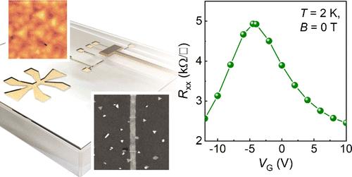
Selective-area epitaxy (SAE) is a useful technique to grow epitaxial films with a desired shape on a prepatterned substrate. Although SAE of patterned topological-insulator (TI) thin films has been performed in the past, there has been no report of SAE-grown TI structures that are bulk-insulating. Here we report the successful growth of Hall-bars and nanowires of bulk-insulating TIs using the SAE technique. Their transport properties show that the quality of the selectively grown structures is comparable to that of bulk-insulating TI films grown on pristine substrates. In SAE-grown TI nanowires, we were able to observe Aharonov–Bohm-like magnetoresistance oscillations that are characteristic of the quantum-confined topological surface states. The availability of bulk-insulating TI nanostructures via the SAE technique opens the possibility to fabricate intricate topological devices in a scalable manner.
中文翻译:

通过分子束外延对体绝缘 (BixSb1–x)2Te3 薄膜和纳米线进行选择性区域外延
选择性区域外延 (SAE) 是一种在预图案化基板上生长具有所需形状的外延薄膜的有用技术。尽管过去已经进行了图案化拓扑绝缘体 (TI) 薄膜的 SAE,但尚未有关于 SAE 生长的体绝缘 TI 结构的报道。在这里,我们报告了使用 SAE 技术成功生长体绝缘 TI 的霍尔棒和纳米线。它们的传输特性表明,选择性生长的结构的质量与在原始基板上生长的体绝缘TI薄膜的质量相当。在 SAE 生长的 TI 纳米线中,我们能够观察到类阿哈罗诺夫-玻姆磁阻振荡,这是量子限制拓扑表面态的特征。通过 SAE 技术获得的体绝缘 TI 纳米结构为以可扩展的方式制造复杂的拓扑器件提供了可能性。
更新日期:2024-07-25
中文翻译:
通过分子束外延对体绝缘 (BixSb1–x)2Te3 薄膜和纳米线进行选择性区域外延
选择性区域外延 (SAE) 是一种在预图案化基板上生长具有所需形状的外延薄膜的有用技术。尽管过去已经进行了图案化拓扑绝缘体 (TI) 薄膜的 SAE,但尚未有关于 SAE 生长的体绝缘 TI 结构的报道。在这里,我们报告了使用 SAE 技术成功生长体绝缘 TI 的霍尔棒和纳米线。它们的传输特性表明,选择性生长的结构的质量与在原始基板上生长的体绝缘TI薄膜的质量相当。在 SAE 生长的 TI 纳米线中,我们能够观察到类阿哈罗诺夫-玻姆磁阻振荡,这是量子限制拓扑表面态的特征。通过 SAE 技术获得的体绝缘 TI 纳米结构为以可扩展的方式制造复杂的拓扑器件提供了可能性。


 京公网安备 11010802027423号