当前位置:
X-MOL 学术
›
ACS Appl. Mater. Interfaces
›
论文详情
Our official English website, www.x-mol.net, welcomes your
feedback! (Note: you will need to create a separate account there.)
Electrostatic Force-Assisted Transfer of Flexible Silicon Photodetector Focal Plane Arrays for Image Sensors
ACS Applied Materials & Interfaces ( IF 8.3 ) Pub Date : 2024-07-22 , DOI: 10.1021/acsami.4c05890 Yuting Ye 1, 2, 3 , Qingyan Deng 2, 3 , Jianghong Wu 2, 3 , Chuyu Zhong 4 , Hui Ma 4 , Yilin Shi 2, 3 , Dingwei Li 2, 3 , Renjie Tang 2, 3 , Yiheng Tang 2, 3 , Jialing Jian 2, 3 , Bowen Zhu 2, 3, 5 , Hongtao Lin 4 , Lan Li 2, 3, 5
ACS Applied Materials & Interfaces ( IF 8.3 ) Pub Date : 2024-07-22 , DOI: 10.1021/acsami.4c05890 Yuting Ye 1, 2, 3 , Qingyan Deng 2, 3 , Jianghong Wu 2, 3 , Chuyu Zhong 4 , Hui Ma 4 , Yilin Shi 2, 3 , Dingwei Li 2, 3 , Renjie Tang 2, 3 , Yiheng Tang 2, 3 , Jialing Jian 2, 3 , Bowen Zhu 2, 3, 5 , Hongtao Lin 4 , Lan Li 2, 3, 5
Affiliation
|
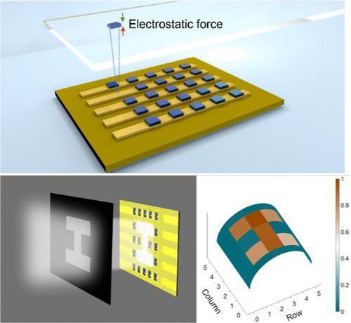
Flexible photodetectors are pivotal in contemporary optoelectronic technology applications, such as data reception and image sensing, yet their performance and yield are often hindered by the challenge of heterogeneous integration between photoactive materials and flexible substrates. Here, we showcase the potential of an electrostatic force-assisted transfer printing technique for integrating Si PIN photodiodes onto flexible substrates. This clean and dry process eliminates the need for chemical etchants, making it a highly desirable method for manufacturing high-performance flexible photodetector arrays, expanding their widespread applications in electronic eyes, robotics, and human–machine interaction. As a demonstration, a 5 × 5 flexible Si photodetector focal plane array is constructed for imaging sensors and shaped into a convex semicylindrical form to achieve a π field of view with long-term mechanical and thermal stability. Such an approach provides a high yield rate and consistent performance, with the single photodetector demonstrating exceptional characteristics, including a responsivity of 0.61 A/W, a response speed of 39.77 MHz, a linear dynamic range of 108.53 dB, and a specific detectivity of 2.75 × 10¹² Jones at an applied voltage of −3 V at 940 nm.
中文翻译:

用于图像传感器的柔性硅光电探测器焦平面阵列的静电力辅助转移
柔性光电探测器在数据接收和图像传感等当代光电技术应用中至关重要,但其性能和产量往往受到光敏材料和柔性基板之间异质集成挑战的阻碍。在这里,我们展示了静电力辅助转印技术将 Si PIN 光电二极管集成到柔性基板上的潜力。这种清洁干燥的工艺无需化学蚀刻剂,使其成为制造高性能柔性光电探测器阵列的理想方法,从而扩展了其在电子眼、机器人和人机交互中的广泛应用。作为演示,为成像传感器构建了 5 × 5 柔性硅光电探测器焦平面阵列,并将其成形为凸半圆柱形,以实现具有长期机械和热稳定性的 π 视场。这种方法提供了高良率和一致的性能,单个光电探测器表现出卓越的特性,包括 0.61 A/W 的响应度、39.77 MHz 的响应速度、108.53 dB 的线性动态范围和 2.75 的比探测率× 10 12 Jones 在 940 nm 处施加 -3 V 电压。
更新日期:2024-07-22
中文翻译:
用于图像传感器的柔性硅光电探测器焦平面阵列的静电力辅助转移
柔性光电探测器在数据接收和图像传感等当代光电技术应用中至关重要,但其性能和产量往往受到光敏材料和柔性基板之间异质集成挑战的阻碍。在这里,我们展示了静电力辅助转印技术将 Si PIN 光电二极管集成到柔性基板上的潜力。这种清洁干燥的工艺无需化学蚀刻剂,使其成为制造高性能柔性光电探测器阵列的理想方法,从而扩展了其在电子眼、机器人和人机交互中的广泛应用。作为演示,为成像传感器构建了 5 × 5 柔性硅光电探测器焦平面阵列,并将其成形为凸半圆柱形,以实现具有长期机械和热稳定性的 π 视场。这种方法提供了高良率和一致的性能,单个光电探测器表现出卓越的特性,包括 0.61 A/W 的响应度、39.77 MHz 的响应速度、108.53 dB 的线性动态范围和 2.75 的比探测率× 10 12 Jones 在 940 nm 处施加 -3 V 电压。


 京公网安备 11010802027423号