当前位置:
X-MOL 学术
›
ACS Appl. Mater. Interfaces
›
论文详情
Our official English website, www.x-mol.net, welcomes your
feedback! (Note: you will need to create a separate account there.)
Microstructure Evolution and Electrical Behaviors for High-Performance Cu2O/Zr-Doped β-Ga2O3 Heterojunction Diodes
ACS Applied Materials & Interfaces ( IF 8.3 ) Pub Date : 2024-07-20 , DOI: 10.1021/acsami.4c06071
Jiangyiming Jiang 1 , Simeng Wu 1 , Peisen Liu 1 , Yun Tian 1
ACS Applied Materials & Interfaces ( IF 8.3 ) Pub Date : 2024-07-20 , DOI: 10.1021/acsami.4c06071
Jiangyiming Jiang 1 , Simeng Wu 1 , Peisen Liu 1 , Yun Tian 1
Affiliation
|
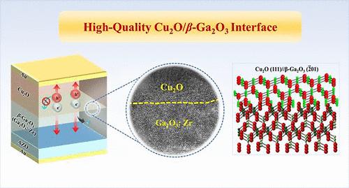
Beta-gallium oxide (β-Ga2O3) is emerging as a promising ultrawide band gap (UWBG) semiconductor, which is vital for high-power, high-frequency electronics and deep-UV optoelectronics. It is especially significant for flexible wearable electronics, enabling the fabrication of high-performance Ga2O3-based devices at low temperatures. However, the limited crystallinity and pronounced structural defects arising from the low-temperature deposition of Ga2O3 films significantly restrict the heterojunction interface quality and the relevant electrical performance of Ga2O3-based devices. In this work, cuprous oxide (Cu2O)/Zr-doped β-Ga2O3 heterojunction diodes are fabricated by magnetron sputtering without intentional substrate heating, followed by an investigation into their microstructure and electrical behaviors. Zr doping can markedly enhance the Ga2O3 crystallinity at low substrate temperatures, transforming the amorphous structure of pristine Ga2O3 films into the crystallized β phase. Moreover, crystalline β-Ga2O3 facilitates the epitaxial growth of the Cu2O phase, suppressing the formation of detrimental secondary phase CuO at the heterojunction interface. Benefiting from the high-quality heterojunction interface, the Cu2O/Zr-doped β-Ga2O3 heterojunction diode exhibits a near-ideal electrical behavior with a low ideality factor of 1.6. The consistent electrical parameters extracted from current–voltage (J–V) and capacitance–voltage (C–V) measurements also confirm the high quality of β-Ga2O3. This work highlights the potential for the low-temperature production of high-quality β-Ga2O3-based heterojunction devices through Zr doping.
中文翻译:

高性能 Cu2O/Zr 掺杂 β-Ga2O3 异质结二极管的微观结构演变和电学行为
β-氧化镓 (β-Ga 2 O 3 ) 正在成为一种有前景的超宽带隙 (UWBG) 半导体,对于高功率、高频电子和深紫外光电子至关重要。它对于柔性可穿戴电子产品尤其重要,可以在低温下制造高性能 Ga 2 O 3基器件。然而,Ga 2 O 3薄膜低温沉积产生的有限结晶度和明显的结构缺陷严重限制了异质结界面质量和Ga 2 O 3基器件的相关电性能。在这项工作中,氧化亚铜(Cu 2 O)/Zr掺杂的β-Ga 2 O 3异质结二极管是通过磁控溅射制造的,无需有意加热基板,然后研究其微观结构和电学行为。 Zr掺杂可以显着提高Ga 2 O 3在低衬底温度下的结晶度,将原始Ga 2 O 3薄膜的非晶结构转变为结晶β相。此外,结晶β-Ga 2 O 3促进Cu 2 O相的外延生长,抑制异质结界面处有害的第二相CuO的形成。得益于高质量的异质结界面,Cu 2 O/Zr掺杂的β-Ga 2 O 3异质结二极管表现出接近理想的电学行为,理想因子低至1.6。 从电流-电压( J-V )和电容-电压( C-V )测量中提取的一致的电学参数也证实了β-Ga 2 O 3的高质量。这项工作凸显了通过 Zr 掺杂低温生产高质量 β-Ga 2 O 3基异质结器件的潜力。
更新日期:2024-07-20
中文翻译:
高性能 Cu2O/Zr 掺杂 β-Ga2O3 异质结二极管的微观结构演变和电学行为
β-氧化镓 (β-Ga 2 O 3 ) 正在成为一种有前景的超宽带隙 (UWBG) 半导体,对于高功率、高频电子和深紫外光电子至关重要。它对于柔性可穿戴电子产品尤其重要,可以在低温下制造高性能 Ga 2 O 3基器件。然而,Ga 2 O 3薄膜低温沉积产生的有限结晶度和明显的结构缺陷严重限制了异质结界面质量和Ga 2 O 3基器件的相关电性能。在这项工作中,氧化亚铜(Cu 2 O)/Zr掺杂的β-Ga 2 O 3异质结二极管是通过磁控溅射制造的,无需有意加热基板,然后研究其微观结构和电学行为。 Zr掺杂可以显着提高Ga 2 O 3在低衬底温度下的结晶度,将原始Ga 2 O 3薄膜的非晶结构转变为结晶β相。此外,结晶β-Ga 2 O 3促进Cu 2 O相的外延生长,抑制异质结界面处有害的第二相CuO的形成。得益于高质量的异质结界面,Cu 2 O/Zr掺杂的β-Ga 2 O 3异质结二极管表现出接近理想的电学行为,理想因子低至1.6。 从电流-电压( J-V )和电容-电压( C-V )测量中提取的一致的电学参数也证实了β-Ga 2 O 3的高质量。这项工作凸显了通过 Zr 掺杂低温生产高质量 β-Ga 2 O 3基异质结器件的潜力。


 京公网安备 11010802027423号