当前位置:
X-MOL 学术
›
Adv. Mater.
›
论文详情
Our official English website, www.x-mol.net, welcomes your feedback! (Note: you will need to create a separate account there.)
Enhanced SWIR Light Detection in Organic Semiconductor Photodetectors through Up‐Conversion of Mid‐Gap Trap States
Advanced Materials ( IF 27.4 ) Pub Date : 2024-07-24 , DOI: 10.1002/adma.202405061 Stefan Zeiske 1, 2 , Nasim Zarrabi 1 , Oskar J. Sandberg 1, 3 , Sam Gielen 4, 5 , Wouter Maes 4, 5 , Paul Meredith 1 , Ardalan Armin 1
Advanced Materials ( IF 27.4 ) Pub Date : 2024-07-24 , DOI: 10.1002/adma.202405061 Stefan Zeiske 1, 2 , Nasim Zarrabi 1 , Oskar J. Sandberg 1, 3 , Sam Gielen 4, 5 , Wouter Maes 4, 5 , Paul Meredith 1 , Ardalan Armin 1
Affiliation
|
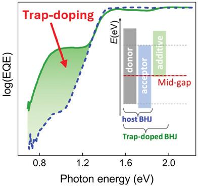
Shortwave‐infrared (SWIR) photodetectors are vital for many scientific and industrial applications including surveillance, quality control and inspection. In recent decades, photodetectors based on organic semiconductors have emerged, demonstrating potential to add real value to broadband and narrowband imaging and sensing scenarios, where factors such as thermal budget sensitivity, large area aperture necessity, cost considerations, and lightweight and conformal flexibility demands are prioritized. It is now recognized that the performance of organic photodetectors (OPDs), notably their specific detectivity, is ultimately limited by trap states, universally present in disordered semiconductors. This work adopts an approach of utilizing these mid‐gap states to specifically create a SWIR photo‐response. To this end, this work introduces a somewhat counter‐intuitive approach of “trap‐doping” in bulk heterojunction (BHJs) photodiodes, where small quantities of a guest organic molecule are intentionally incorporated into a semiconducting donor:acceptor host system. Following this approach, this work demonstrates a proof‐of‐concept for a visible‐to‐SWIR broadband OPD, approaching (and, to some extent, even exceeding) state‐of‐the‐art performance across critical photodetector metrics. The trap‐doping approach is, even though only a proof‐of‐concept currently, broadly applicable to various spectral windows. It represents a new modality for engineering photodetection using the unconventional strategy of turning a limitation into a feature.
中文翻译:

通过中带隙陷阱态的上转换增强有机半导体光电探测器中的短波红外光检测
短波红外 (SWIR) 光电探测器对于许多科学和工业应用(包括监视、质量控制和检查)至关重要。近几十年来,基于有机半导体的光电探测器已经出现,展示了为宽带和窄带成像和传感场景增加真正价值的潜力,其中热预算敏感性、大面积孔径必要性、成本考虑以及轻质和共形灵活性需求等因素是优先。现在人们认识到,有机光电探测器(OPD)的性能,尤其是它们的比探测率,最终受到普遍存在于无序半导体中的陷阱态的限制。这项工作采用了利用这些中带隙态来专门创建短波红外光响应的方法。为此,这项工作在体异质结(BHJ)光电二极管中引入了一种有点反直觉的“陷阱掺杂”方法,其中少量的客体有机分子被有意地纳入半导体供体:受体主体系统中。采用这种方法,这项工作展示了可见光到短波红外宽带 OPD 的概念验证,在关键光电探测器指标上接近(甚至在某种程度上甚至超过)最先进的性能。陷阱掺杂方法尽管目前只是概念验证,但广泛适用于各种光谱窗口。它代表了一种利用将限制转变为特征的非常规策略的光电检测工程新模式。
更新日期:2024-07-24
中文翻译:
通过中带隙陷阱态的上转换增强有机半导体光电探测器中的短波红外光检测
短波红外 (SWIR) 光电探测器对于许多科学和工业应用(包括监视、质量控制和检查)至关重要。近几十年来,基于有机半导体的光电探测器已经出现,展示了为宽带和窄带成像和传感场景增加真正价值的潜力,其中热预算敏感性、大面积孔径必要性、成本考虑以及轻质和共形灵活性需求等因素是优先。现在人们认识到,有机光电探测器(OPD)的性能,尤其是它们的比探测率,最终受到普遍存在于无序半导体中的陷阱态的限制。这项工作采用了利用这些中带隙态来专门创建短波红外光响应的方法。为此,这项工作在体异质结(BHJ)光电二极管中引入了一种有点反直觉的“陷阱掺杂”方法,其中少量的客体有机分子被有意地纳入半导体供体:受体主体系统中。采用这种方法,这项工作展示了可见光到短波红外宽带 OPD 的概念验证,在关键光电探测器指标上接近(甚至在某种程度上甚至超过)最先进的性能。陷阱掺杂方法尽管目前只是概念验证,但广泛适用于各种光谱窗口。它代表了一种利用将限制转变为特征的非常规策略的光电检测工程新模式。


 京公网安备 11010802027423号