当前位置:
X-MOL 学术
›
J. Am. Chem. Soc.
›
论文详情
Our official English website, www.x-mol.net, welcomes your feedback! (Note: you will need to create a separate account there.)
Epitaxial Integration of Transferable High-κ Dielectric and 2D Semiconductor
Journal of the American Chemical Society ( IF 14.4 ) Pub Date : 2024-07-22 , DOI: 10.1021/jacs.4c04984 Xuzhong Cong 1 , Xiaoyin Gao 1 , Haoying Sun 2 , Xuehan Zhou 1 , Yongchao Zhu 1 , Xin Gao 1 , Congwei Tan 1 , Jingyue Wang 1 , Leyan Nian 3 , Yuefeng Nie 2 , Hailin Peng 1
Journal of the American Chemical Society ( IF 14.4 ) Pub Date : 2024-07-22 , DOI: 10.1021/jacs.4c04984 Xuzhong Cong 1 , Xiaoyin Gao 1 , Haoying Sun 2 , Xuehan Zhou 1 , Yongchao Zhu 1 , Xin Gao 1 , Congwei Tan 1 , Jingyue Wang 1 , Leyan Nian 3 , Yuefeng Nie 2 , Hailin Peng 1
Affiliation
|
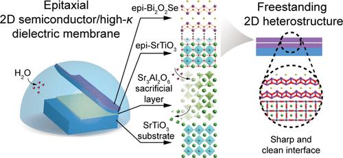
The synthesis of high-dielectric-constant (high-κ) dielectric materials and their integration with channel materials have been the key challenges in the state-of-the-art transistor architecture, as they can provide strong gate control and low operating voltage. For next-generation electronics, high-mobility two-dimensional (2D) layered semiconductors with dangling-bond-free surfaces and an atomic-thick thickness are being explored as channel materials to achieve shorter channel lengths and less interfacial scattering. Nowadays, the integration of high-κ dielectrics with high-mobility 2D semiconductors mainly relies on atomic layer deposition or transfer stacking, which may cause several undesirable problems, such as channel damage and interface traps. Here, we demonstrate the integration of high-mobility 2D semiconducting Bi2O2Se with transferable high-κ SrTiO3 as a 2D field-effect transistor by direct epitaxial growth. Remarkably, such 2D heterostructures can be efficiently transferred from the water-soluble Sr3Al2O6 sacrificial layer onto arbitrary substrates. The as-fabricated 2D Bi2O2Se/SrTiO3 transistors exhibit an on/off ratio over 104 and a subthreshold swing down to 90 mV/dec. Furthermore, the 2D Bi2O2Se/SrTiO3 heterostructures can be easily transferred onto flexible polyethylene terephthalate (PET) substrates, and the as-fabricated transistors exhibit good potential in flexible electronics. Our study opens up a new avenue for the integration of high-κ dielectrics with high-mobility 2D semiconductors and paves the way for the exploration of multifunctional electronic devices.
中文翻译:

可转移高κ电介质和二维半导体的外延集成
高介电常数(高κ)介电材料的合成及其与沟道材料的集成一直是最先进的晶体管架构的关键挑战,因为它们可以提供强大的栅极控制和低工作电压。对于下一代电子产品,正在探索具有无悬挂键表面和原子厚厚度的高迁移率二维(2D)层状半导体作为沟道材料,以实现更短的沟道长度和更少的界面散射。目前,高κ电介质与高迁移率二维半导体的集成主要依赖于原子层沉积或转移堆叠,这可能会导致一些不良问题,例如沟道损伤和界面陷阱。在这里,我们展示了高迁移率二维半导体 Bi 2 O 2 Se 与可转移高 K SrTiO 3 的集成作为二维场效应晶体管:直接外延生长。值得注意的是,这种二维异质结构可以有效地从水溶性Sr 3 Al 2 O 6 牺牲层转移到任意基板上。所制造的 2D Bi 2 O 2 Se/SrTiO 3 晶体管表现出超过 10 4 的开/关比和亚阈值摆幅降至 90 mV/dec。此外,2D Bi 2 O 2 Se/SrTiO 3 异质结构可以轻松转移到柔性聚对苯二甲酸乙二醇酯(PET)基板上,并且所制造的晶体管在柔性电子领域展现出良好的潜力。我们的研究为高κ电介质与高迁移率二维半导体的集成开辟了一条新途径,并为多功能电子器件的探索铺平了道路。
更新日期:2024-07-23
中文翻译:
可转移高κ电介质和二维半导体的外延集成
高介电常数(高κ)介电材料的合成及其与沟道材料的集成一直是最先进的晶体管架构的关键挑战,因为它们可以提供强大的栅极控制和低工作电压。对于下一代电子产品,正在探索具有无悬挂键表面和原子厚厚度的高迁移率二维(2D)层状半导体作为沟道材料,以实现更短的沟道长度和更少的界面散射。目前,高κ电介质与高迁移率二维半导体的集成主要依赖于原子层沉积或转移堆叠,这可能会导致一些不良问题,例如沟道损伤和界面陷阱。在这里,我们展示了高迁移率二维半导体 Bi 2 O 2 Se 与可转移高 K SrTiO 3 的集成作为二维场效应晶体管:直接外延生长。值得注意的是,这种二维异质结构可以有效地从水溶性Sr 3 Al 2 O 6 牺牲层转移到任意基板上。所制造的 2D Bi 2 O 2 Se/SrTiO 3 晶体管表现出超过 10 4 的开/关比和亚阈值摆幅降至 90 mV/dec。此外,2D Bi 2 O 2 Se/SrTiO 3 异质结构可以轻松转移到柔性聚对苯二甲酸乙二醇酯(PET)基板上,并且所制造的晶体管在柔性电子领域展现出良好的潜力。我们的研究为高κ电介质与高迁移率二维半导体的集成开辟了一条新途径,并为多功能电子器件的探索铺平了道路。


 京公网安备 11010802027423号