Nature Nanotechnology ( IF 38.1 ) Pub Date : 2024-07-10 , DOI: 10.1038/s41565-024-01704-3 Can Liu 1, 2 , Tianyao Liu 1 , Zhibin Zhang 1 , Zhipei Sun 3 , Guangyu Zhang 4, 5 , Enge Wang 4, 6 , Kaihui Liu 1, 4, 7
|
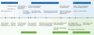
The exceptional physical properties of two-dimensional (2D) van der Waals (vdW) materials have been extensively researched, driving advances in material synthesis. Epitaxial growth, a prominent synthesis strategy, enables the production of large-area, high-quality 2D films compatible with advanced integrated circuits. Typical 2D single crystals, such as graphene, transition metal dichalcogenides and hexagonal boron nitride, have been epitaxially grown at a wafer scale. A systematic summary is required to offer strategic guidance for the epitaxy of emerging 2D materials. Here we focus on the epitaxy methodologies for 2D vdW materials in two directions: the growth of in-plane single-crystal monolayers and the fabrication of out-of-plane homostructures. We first discuss nucleation control of a single domain and orientation control over multiple domains to achieve large-scale single-crystal monolayers. We analyse the defect levels and measures of crystalline quality of typical 2D vdW materials with various epitaxial growth techniques. We then outline technical routes for the growth of homogeneous multilayers and twisted homostructures. We further summarize the current strategies to guide future efforts in optimizing on-demand fabrication of 2D vdW materials, as well as subsequent device manufacturing for their industrial applications.
中文翻译:
了解二维材料及其同质结构的外延生长
二维 (2D) 范德华 (vdW) 材料的卓越物理性质已得到广泛研究,推动了材料合成的进步。外延生长是一种重要的合成策略,可以生产与先进集成电路兼容的大面积、高质量的 2D 薄膜。典型的二维单晶,例如石墨烯、过渡金属二硫属化物和六方氮化硼,已经在晶圆级外延生长。需要系统总结来为新兴二维材料的外延提供战略指导。在这里,我们重点关注两个方向的二维 vdW 材料的外延方法:面内单晶单层的生长和面外同质结构的制造。我们首先讨论单域的成核控制和多个域的取向控制,以实现大规模单晶单层。我们分析了采用各种外延生长技术的典型 2D vdW 材料的缺陷水平和晶体质量测量。然后,我们概述了同质多层和扭曲同质结构生长的技术路线。我们进一步总结了当前的策略,以指导未来优化 2D vdW 材料的按需制造及其工业应用的后续设备制造的工作。


 京公网安备 11010802027423号