Light: Science & Applications ( IF 20.6 ) Pub Date : 2024-07-08 , DOI: 10.1038/s41377-024-01503-4 Debapam Bose 1 , Mark W Harrington 1 , Andrei Isichenko 1 , Kaikai Liu 1 , Jiawei Wang 1 , Nitesh Chauhan 1 , Zachary L Newman 2 , Daniel J Blumenthal 1
|
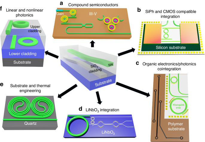
Heterogeneous and monolithic integration of the versatile low-loss silicon nitride platform with low-temperature materials such as silicon electronics and photonics, III–V compound semiconductors, lithium niobate, organics, and glasses has been inhibited by the need for high-temperature annealing as well as the need for different process flows for thin and thick waveguides. New techniques are needed to maintain the state-of-the-art losses, nonlinear properties, and CMOS-compatible processes while enabling this next generation of 3D silicon nitride integration. We report a significant advance in silicon nitride integrated photonics, demonstrating the lowest losses to date for an anneal-free process at a maximum temperature 250 °C, with the same deuterated silane based fabrication flow, for nitride and oxide, for an order of magnitude range in nitride thickness without requiring stress mitigation or polishing. We report record low anneal-free losses for both nitride core and oxide cladding, enabling 1.77 dB m-1 loss and 14.9 million Q for 80 nm nitride core waveguides, more than half an order magnitude lower loss than previously reported sub 300 °C process. For 800 nm-thick nitride, we achieve as good as 8.66 dB m−1 loss and 4.03 million Q, the highest reported Q for a low temperature processed resonator with equivalent device area, with a median of loss and Q of 13.9 dB m−1 and 2.59 million each respectively. We demonstrate laser stabilization with over 4 orders of magnitude frequency noise reduction using a thin nitride reference cavity, and using a thick nitride micro-resonator we demonstrate OPO, over two octave supercontinuum generation, and four-wave mixing and parametric gain with the lowest reported optical parametric oscillation threshold per unit resonator length. These results represent a significant step towards a uniform ultra-low loss silicon nitride homogeneous and heterogeneous platform for both thin and thick waveguides capable of linear and nonlinear photonic circuits and integration with low-temperature materials and processes.
中文翻译:
免退火超低损耗氮化硅集成光子学
多功能低损耗氮化硅平台与硅电子和光子学、III-V族化合物半导体、铌酸锂、有机物和玻璃等低温材料的异质单片集成因高温退火的需要而受到抑制,因为以及薄波导和厚波导对不同工艺流程的需求。需要新技术来保持最先进的损耗、非线性特性和 CMOS 兼容工艺,同时实现下一代 3D 氮化硅集成。我们报告了氮化硅集成光子学的重大进展,展示了迄今为止在最高温度 250 °C 下的免退火工艺的最低损耗,采用相同的基于氘代硅烷的制造流程,对于氮化物和氧化物来说,损耗达到一个数量级氮化物厚度范围内,无需应力减轻或抛光。我们报告氮化物芯和氧化物包层的无退火损耗创历史新低,80 nm 氮化物芯波导的损耗为 1.77 dB m -1 ,Q 值为 1,490 万,比之前报道的低于 300 °C 工艺的损耗低半个数量级以上。对于 800 nm 厚的氮化物,我们实现了高达 8.66 dB m −1的损耗和 403 万 Q 值,这是具有同等器件面积的低温处理谐振器报道的最高 Q 值,损耗和 Q 值的中值为 13.9 dB m −分别为1和 259 万。 我们使用薄氮化物参考腔演示了具有超过 4 个数量级频率噪声降低的激光稳定性,并使用厚氮化物微谐振器演示了 OPO、超过两个倍频程的超连续谱生成以及四波混频和参数增益,具有最低的报告值每单位谐振器长度的光学参量振荡阈值。这些结果代表了朝着用于薄波导和厚波导的均匀超低损耗氮化硅均质和异质平台迈出的重要一步,该平台能够实现线性和非线性光子电路以及与低温材料和工艺的集成。


 京公网安备 11010802027423号