当前位置:
X-MOL 学术
›
Adv. Funct. Mater.
›
论文详情
Our official English website, www.x-mol.net, welcomes your feedback! (Note: you will need to create a separate account there.)
Built-In Electric Field Enhancement Strategy Induced by Cross-Dimensional Nano-Heterointerface Design for Electromagnetic Wave Absorption
Advanced Functional Materials ( IF 18.5 ) Pub Date : 2024-07-01 , DOI: 10.1002/adfm.202407217 Xin Li 1, 2 , Xinlei Wang 1 , Minghang Li 1 , Wenjie Zhu 1 , Haojie Luo 1 , Xiaoke Lu 3 , Hailong Xu 4 , Jimei Xue 1 , Fang Ye 1 , Hongjing Wu 5 , Xiaomeng Fan 1
Advanced Functional Materials ( IF 18.5 ) Pub Date : 2024-07-01 , DOI: 10.1002/adfm.202407217 Xin Li 1, 2 , Xinlei Wang 1 , Minghang Li 1 , Wenjie Zhu 1 , Haojie Luo 1 , Xiaoke Lu 3 , Hailong Xu 4 , Jimei Xue 1 , Fang Ye 1 , Hongjing Wu 5 , Xiaomeng Fan 1
Affiliation
|
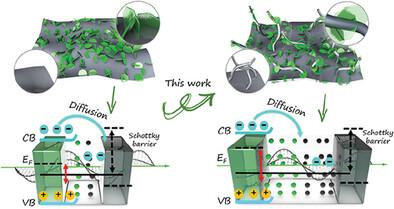
Nano-heterointerface engineering has been demonstrated to influence interfacial polarization by expanding the interface surface area and constructing a built-in electric field (BEF), thus regulating electromagnetic (EM) wave absorption. However, the dielectric-responsive mechanism of the BEF needs further exploration to enhance the comprehensive understanding of interfacial polarization, particularly in terms of quantifying and optimizing the BEF strength. Herein, a “1D expanded 2D structure” carbon matrix is designed, and semiconductor ZnIn2S4 (ZIS) is introduced to construct a carbon/ZIS heterostructure. The cross-dimensional nano-heterointerface design increases interface coupling sites by expanding the interface surface area and induces an increase in the Fermi level difference on both sides of the interface to modulate the distribution of interface charges, thereby strengthening the BEF at the interface. The synergistic effect leads to excellent EM absorption performance (minimum reflection coefficient RCmin = −67.4 dB, effective absorption bandwidth EAB = 6.0 GHz) of carbon/ZIS heterostructure. This work introduces a general modification model for enhancing interfacial polarization and inspires the development of new strategies for EM functional materials with unique electronic behaviors through heterointerface engineering.
中文翻译:

跨维纳米异质界面设计诱导的内置电场增强策略用于电磁波吸收
纳米异质界面工程已被证明可以通过扩大界面表面积和构建内置电场(BEF)来影响界面极化,从而调节电磁(EM)波吸收。然而,BEF的介电响应机制需要进一步探索,以增强对界面极化的全面理解,特别是在量化和优化BEF强度方面。本文设计了“1D扩展2D结构”碳基体,并引入半导体ZnIn 2 S 4 (ZIS)来构建碳/ZIS异质结构。跨维纳米异质界面设计通过扩大界面表面积来增加界面耦合位点,并诱导界面两侧费米能级差的增加来调节界面电荷的分布,从而增强界面处的BEF。协同效应使得碳/ZIS异质结构具有优异的电磁吸收性能(最小反射系数RC min = -67.4 dB,有效吸收带宽EAB = 6.0 GHz)。这项工作介绍了一种增强界面极化的通用改性模型,并激发了通过异质界面工程开发具有独特电子行为的电磁功能材料的新策略。
更新日期:2024-07-01
中文翻译:
跨维纳米异质界面设计诱导的内置电场增强策略用于电磁波吸收
纳米异质界面工程已被证明可以通过扩大界面表面积和构建内置电场(BEF)来影响界面极化,从而调节电磁(EM)波吸收。然而,BEF的介电响应机制需要进一步探索,以增强对界面极化的全面理解,特别是在量化和优化BEF强度方面。本文设计了“1D扩展2D结构”碳基体,并引入半导体ZnIn 2 S 4 (ZIS)来构建碳/ZIS异质结构。跨维纳米异质界面设计通过扩大界面表面积来增加界面耦合位点,并诱导界面两侧费米能级差的增加来调节界面电荷的分布,从而增强界面处的BEF。协同效应使得碳/ZIS异质结构具有优异的电磁吸收性能(最小反射系数RC min = -67.4 dB,有效吸收带宽EAB = 6.0 GHz)。这项工作介绍了一种增强界面极化的通用改性模型,并激发了通过异质界面工程开发具有独特电子行为的电磁功能材料的新策略。


 京公网安备 11010802027423号