当前位置:
X-MOL 学术
›
Adv. Funct. Mater.
›
论文详情
Our official English website, www.x-mol.net, welcomes your feedback! (Note: you will need to create a separate account there.)
Heat Transport at Silicon Grain Boundaries
Advanced Functional Materials ( IF 18.5 ) Pub Date : 2024-07-01 , DOI: 10.1002/adfm.202405413 Eleonora Isotta 1 , Shizhou Jiang 2 , Ruben Bueno‐Villoro 3 , Ryohei Nagahiro 4 , Kosuke Maeda 4 , Dominique Alexander Mattlat 3 , Alesanmi R. Odufisan 5 , Alexandra Zevalkink 6 , Junichiro Shiomi 4, 7 , Siyuan Zhang 3 , Christina Scheu 3 , G. Jeffrey Snyder 1 , Oluwaseyi Balogun 2, 8
Advanced Functional Materials ( IF 18.5 ) Pub Date : 2024-07-01 , DOI: 10.1002/adfm.202405413 Eleonora Isotta 1 , Shizhou Jiang 2 , Ruben Bueno‐Villoro 3 , Ryohei Nagahiro 4 , Kosuke Maeda 4 , Dominique Alexander Mattlat 3 , Alesanmi R. Odufisan 5 , Alexandra Zevalkink 6 , Junichiro Shiomi 4, 7 , Siyuan Zhang 3 , Christina Scheu 3 , G. Jeffrey Snyder 1 , Oluwaseyi Balogun 2, 8
Affiliation
|
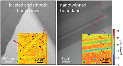
Engineering microstructural defects, like grain boundaries, offers superior control over transport properties in energy materials. However, technological advancement requires establishing microstructure‐property relations at the micron or finer scales, where most of these defects operate. Here, the first experimental evidence of thermal resistance for individual silicon grain boundaries, estimated with a Gibbs excess approach, is provided. Coincident site lattice boundaries exhibit uniform excess thermal resistance along the same boundary, but notable variations from one boundary to another. Boundaries associated with low interface energy generally exhibit lower resistances, aligning with theoretical expectations and previous simulations, but several exceptions are observed. Transmission electron microscopy reveals that factors like interface roughness and presence of nanotwinning can significantly alter the observed resistance, which ranges from ∼0 to up to ∼2.3 m2 K/GW. In stark contrast, significantly larger and less uniform values ‐ from 5 to 30 m2 K/GW ‐ are found for high‐angle boundaries in spark‐plasma‐sintered polycrystalline silicon. Further, finite element analysis suggests that boundary planes that strongly deviate from the sample vertical (beyond ∼45°) can show up to 3‐times larger excess resistance. Direct correlations of properties with individual defects enable the design of materials with superior thermal performance for applications in energy harvesting and heat management.
中文翻译:

硅晶界的热传输
工程微观结构缺陷(例如晶界)可以对能源材料的传输特性进行卓越的控制。然而,技术进步需要在微米或更精细的尺度上建立微观结构-性能关系,而大多数缺陷都是在微米或更精细的尺度上发生的。在这里,提供了使用吉布斯过剩方法估计的单个硅晶界热阻的第一个实验证据。重合位点晶格边界沿同一边界表现出均匀的过剩热阻,但从一个边界到另一个边界存在显着变化。与低界面能相关的边界通常表现出较低的电阻,与理论预期和之前的模拟一致,但也观察到了一些例外情况。透射电子显微镜显示,界面粗糙度和纳米孪晶的存在等因素可以显着改变观察到的电阻,其范围从~0到~2.3 m2K/GW。与此形成鲜明对比的是,火花等离子体烧结多晶硅中的高角度边界具有明显更大且不太均匀的值(从 5 到 30 m2K/GW)。此外,有限元分析表明,强烈偏离样本垂直方向(超过~45°)的边界面可能会显示出高达 3 倍的额外阻力。性能与单个缺陷的直接相关性使得能够设计出具有优异热性能的材料,用于能量收集和热管理应用。
更新日期:2024-07-01
中文翻译:
硅晶界的热传输
工程微观结构缺陷(例如晶界)可以对能源材料的传输特性进行卓越的控制。然而,技术进步需要在微米或更精细的尺度上建立微观结构-性能关系,而大多数缺陷都是在微米或更精细的尺度上发生的。在这里,提供了使用吉布斯过剩方法估计的单个硅晶界热阻的第一个实验证据。重合位点晶格边界沿同一边界表现出均匀的过剩热阻,但从一个边界到另一个边界存在显着变化。与低界面能相关的边界通常表现出较低的电阻,与理论预期和之前的模拟一致,但也观察到了一些例外情况。透射电子显微镜显示,界面粗糙度和纳米孪晶的存在等因素可以显着改变观察到的电阻,其范围从~0到~2.3 m2K/GW。与此形成鲜明对比的是,火花等离子体烧结多晶硅中的高角度边界具有明显更大且不太均匀的值(从 5 到 30 m2K/GW)。此外,有限元分析表明,强烈偏离样本垂直方向(超过~45°)的边界面可能会显示出高达 3 倍的额外阻力。性能与单个缺陷的直接相关性使得能够设计出具有优异热性能的材料,用于能量收集和热管理应用。


 京公网安备 11010802027423号