当前位置:
X-MOL 学术
›
Adv. Electron. Mater.
›
论文详情
Our official English website, www.x-mol.net, welcomes your feedback! (Note: you will need to create a separate account there.)
Enhancement of Thermal Boundary Conductance between MoS2 and Dielectric Layer by Self‐Assembled Monolayers
Advanced Electronic Materials ( IF 5.3 ) Pub Date : 2024-06-29 , DOI: 10.1002/aelm.202400244 Jian Huang 1 , Xiaotong Yu 2 , Xiaofeng Wang 3 , Fanfan Wang 1 , Zexin Liu 4 , Kai Yang 1 , Yue Yue 4 , Kangyong Li 1 , Ruiwen Dai 3 , Aming Lin 5 , Yiyang Sun 5 , Tianlong Zhao 6 , Zhiqiang Wang 7 , Yuan Gao 2 , Lifu Zhang 8 , Dongdong Chen 6 , Guoqing Xin 1
Advanced Electronic Materials ( IF 5.3 ) Pub Date : 2024-06-29 , DOI: 10.1002/aelm.202400244 Jian Huang 1 , Xiaotong Yu 2 , Xiaofeng Wang 3 , Fanfan Wang 1 , Zexin Liu 4 , Kai Yang 1 , Yue Yue 4 , Kangyong Li 1 , Ruiwen Dai 3 , Aming Lin 5 , Yiyang Sun 5 , Tianlong Zhao 6 , Zhiqiang Wang 7 , Yuan Gao 2 , Lifu Zhang 8 , Dongdong Chen 6 , Guoqing Xin 1
Affiliation
|
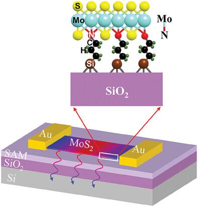
The 2D semiconductor monolayer MoS2 is expected to be a potential channel material to achieve higher miniaturization and integration in post‐Moore era due to its exceptional electrical and optical properties. However, the weak van der Waals interaction between MoS2 and the dielectric substrate induces high interfacial thermal resistance and impedes the heat dissipation, leading to significant temperature rise and consequential device performance degradation. Here, self‐assembled monolayers (SAM) are employed to modify the surface of dielectric SiO2 and enhance thermal boundary conductance (TBC) between MoS2 and dielectric layer. The surface roughness of dielectric SiO2 is improved by the SAM, depressing the photon scattering. More importantly, the interfacial bonding force is strengthened by the formation of chemical covalent N‐Mo bonds between NH2 ‐terminated SAM and MoS2, thus leading to a 118% TBC improvement between MoS2 and NH2 ‐terminated SiO2 compared to pristine SiO2 substrate. Simultaneously, the current reduction caused by self‐heating effect in the monolayer MoS2 field‐effect transistor is eliminated and the maximum power density of the device is largely improved. The incorporation of SAM in 2D semiconductor nanoelectronics presents great potential for device thermal management and reliability improvement.
中文翻译:

自组装单分子层增强MoS2和介电层之间的热边界电导
二维半导体单层MoS2由于其优异的电学和光学特性,有望成为后摩尔时代实现更高小型化和集成化的潜在通道材料。然而,MoS2 和介电基板之间的弱范德华相互作用会导致较高的界面热阻并阻碍散热,导致显着的温升和随之而来的器件性能下降。这里,采用自组装单层(SAM)来修饰电介质 SiO2 的表面并增强 MoS2 和电介质层之间的热边界传导(TBC)。 SAM 改善了电介质 SiO2 的表面粗糙度,抑制了光子散射。更重要的是,通过在 NH2 封端的 SAM 和 MoS2 之间形成化学共价 N-Mo 键,界面结合力得到加强,从而导致 MoS2 和 NH2 封端的 SiO2 之间的 TBC 与原始 SiO2 基材相比提高了 118%。同时,消除了单层MoS2场效应晶体管中自热效应引起的电流降低,大大提高了器件的最大功率密度。将 SAM 纳入 2D 半导体纳米电子学中,为器件热管理和可靠性改进带来了巨大潜力。
更新日期:2024-06-29
中文翻译:
自组装单分子层增强MoS2和介电层之间的热边界电导
二维半导体单层MoS2由于其优异的电学和光学特性,有望成为后摩尔时代实现更高小型化和集成化的潜在通道材料。然而,MoS2 和介电基板之间的弱范德华相互作用会导致较高的界面热阻并阻碍散热,导致显着的温升和随之而来的器件性能下降。这里,采用自组装单层(SAM)来修饰电介质 SiO2 的表面并增强 MoS2 和电介质层之间的热边界传导(TBC)。 SAM 改善了电介质 SiO2 的表面粗糙度,抑制了光子散射。更重要的是,通过在 NH2 封端的 SAM 和 MoS2 之间形成化学共价 N-Mo 键,界面结合力得到加强,从而导致 MoS2 和 NH2 封端的 SiO2 之间的 TBC 与原始 SiO2 基材相比提高了 118%。同时,消除了单层MoS2场效应晶体管中自热效应引起的电流降低,大大提高了器件的最大功率密度。将 SAM 纳入 2D 半导体纳米电子学中,为器件热管理和可靠性改进带来了巨大潜力。


 京公网安备 11010802027423号