当前位置:
X-MOL 学术
›
ACS Appl. Mater. Interfaces
›
论文详情
Our official English website, www.x-mol.net, welcomes your feedback! (Note: you will need to create a separate account there.)
Ultrahigh Bipolar Photoresponse in a Self-Powered Ultraviolet Photodetector Based on GaN and In/Sn-Doped Ga2O3 Nanowires pn junction
ACS Applied Materials & Interfaces ( IF 8.3 ) Pub Date : 2024-06-27 , DOI: 10.1021/acsami.4c04812 Wei Xu 1, 2, 3 , Bei Li 1 , Yutong Wu 1 , Zhiyu Dong 1 , Kun Zhang 1 , Qingshan Wang 4 , Shuanglong Feng 1, 2 , Wenqiang Lu 1, 2
ACS Applied Materials & Interfaces ( IF 8.3 ) Pub Date : 2024-06-27 , DOI: 10.1021/acsami.4c04812 Wei Xu 1, 2, 3 , Bei Li 1 , Yutong Wu 1 , Zhiyu Dong 1 , Kun Zhang 1 , Qingshan Wang 4 , Shuanglong Feng 1, 2 , Wenqiang Lu 1, 2
Affiliation
|
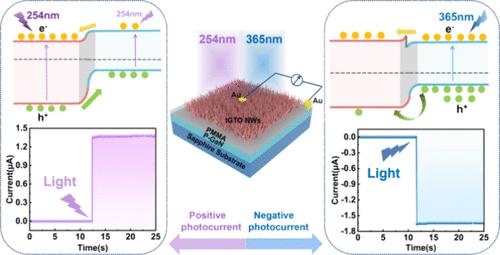
Self-powered ultraviolet photodetectors with bipolar photoresponse have great potential in the fields of ultraviolet optical communication, all-optical controlled artificial synapses, high-resolution ultraviolet imaging equipment, and multiband photoelectric detection. However, the current low optoelectronic performance limits the development of such polar switching devices. Here, we construct a self-powered ultraviolet photodetector based on GaN and In/Sn-doped Ga2O3 (IGTO) nanowires (NWs) pn junction structure. This unique nanowire/thin film structure allows GaN and IGTO to dominate the absorption of light at different wavelengths, resulting in a highly bipolar photoresponse. The device has a responsivity of 2.04 A/W and a normalized detectivity of 7.18 × 10¹³ Jones at 254 nm and a responsivity of −2.09 A/W and a normalized detectivity of −7 × 10¹³ Jones at 365 nm, both at zero bias. In addition, it has an extremely high Ilight/Idark ratio of 1.05 × 10⁵ and ultrafast response times of 2.4/1.9 ms (at 254 nm) and 5.7/5.2 ms (at 365 nm). These excellent properties are attributed to the high specific surface area of the one-dimensional nanowire structure and the abundant voids generated by the nanowire network to enhance the absorption of light, and the p–n junction structure enables the rapid separation and transfer of photogenerated electron–hole pairs. Our findings provide a feasible strategy for high-performance wavelength-controlled polarity switching devices.
中文翻译:

基于 GaN 和 In/Sn 掺杂 Ga2O3 纳米线 pn 结的自供电紫外光电探测器中的超高双极光响应
具有双极光响应的自供电紫外光电探测器在紫外光通信、全光控人工突触、高分辨率紫外成像设备和多波段光电探测等领域具有巨大潜力。然而,目前较低的光电性能限制了此类极性开关器件的发展。在这里,我们构建了一种基于 GaN 和 In/Sn 掺杂 Ga 2 O 3 (IGTO) 纳米线 (NWs) pn 结结构的自供电紫外光电探测器。这种独特的纳米线/薄膜结构使 GaN 和 IGTO 能够主导不同波长的光吸收,从而产生高度双极光响应。该器件在 254 nm 处的响应率为 2.04 A/W,归一化探测率为 7.18 × 10 13 Jones,响应率为 -2.09 A/W,归一化探测率为 -7 × 10 13 琼斯在 365 nm 处,均处于零偏压。此外,它还具有 1.05 × 10 5 的极高 I light /I dark 比率和 2.4/1.9 ms 的超快响应时间(在 254 nm 处) )和 5.7/5.2 毫秒(365 nm)。这些优异的性能归功于一维纳米线结构的高比表面积以及纳米线网络产生的丰富的空隙增强了对光的吸收,而p-n结结构使得光生电子能够快速分离和转移– 孔对。我们的研究结果为高性能波长控制极性切换器件提供了可行的策略。
更新日期:2024-06-27
中文翻译:
基于 GaN 和 In/Sn 掺杂 Ga2O3 纳米线 pn 结的自供电紫外光电探测器中的超高双极光响应
具有双极光响应的自供电紫外光电探测器在紫外光通信、全光控人工突触、高分辨率紫外成像设备和多波段光电探测等领域具有巨大潜力。然而,目前较低的光电性能限制了此类极性开关器件的发展。在这里,我们构建了一种基于 GaN 和 In/Sn 掺杂 Ga 2 O 3 (IGTO) 纳米线 (NWs) pn 结结构的自供电紫外光电探测器。这种独特的纳米线/薄膜结构使 GaN 和 IGTO 能够主导不同波长的光吸收,从而产生高度双极光响应。该器件在 254 nm 处的响应率为 2.04 A/W,归一化探测率为 7.18 × 10 13 Jones,响应率为 -2.09 A/W,归一化探测率为 -7 × 10 13 琼斯在 365 nm 处,均处于零偏压。此外,它还具有 1.05 × 10 5 的极高 I light /I dark 比率和 2.4/1.9 ms 的超快响应时间(在 254 nm 处) )和 5.7/5.2 毫秒(365 nm)。这些优异的性能归功于一维纳米线结构的高比表面积以及纳米线网络产生的丰富的空隙增强了对光的吸收,而p-n结结构使得光生电子能够快速分离和转移– 孔对。我们的研究结果为高性能波长控制极性切换器件提供了可行的策略。


 京公网安备 11010802027423号