当前位置:
X-MOL 学术
›
ACS Appl. Mater. Interfaces
›
论文详情
Our official English website, www.x-mol.net, welcomes your feedback! (Note: you will need to create a separate account there.)
Localized Surface Doping Induced Ultralow Contact Resistance between Metal and (Bi,Sb)2Te3 Thermoelectric Films
ACS Applied Materials & Interfaces ( IF 8.3 ) Pub Date : 2024-06-27 , DOI: 10.1021/acsami.4c06713 Man Zhou 1 , Wei Zhu 1, 2 , Shucheng Bao 1 , Jie Zhou 1 , Yuedong Yu 1 , Qingqing Zhang 2 , Chaojie Ren 1 , Zhi Li 1 , Yuan Deng 1, 2
ACS Applied Materials & Interfaces ( IF 8.3 ) Pub Date : 2024-06-27 , DOI: 10.1021/acsami.4c06713 Man Zhou 1 , Wei Zhu 1, 2 , Shucheng Bao 1 , Jie Zhou 1 , Yuedong Yu 1 , Qingqing Zhang 2 , Chaojie Ren 1 , Zhi Li 1 , Yuan Deng 1, 2
Affiliation
|
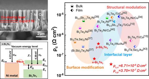
Micro thermoelectric devices are expected to further improve the cooling density for the temperature control of electronic devices; nevertheless, the high contact resistivity between metals and semiconductors critically limits their applications, especially in chip cooling with extremely high heat flux. Herein, based on the calculated results, a low specific contact resistivity of ∼10–7 Ω cm2 at the interface is required to guarantee a desirable cooling power density of micro devices. Thus, we developed a generally applicable interfacial modulation strategy via localized surface doping of thermoelectric films, and the feasibility of such a doping approach for both n/p-type (Bi,Sb)2Te3 films was demonstrated, which can effectively increase the surface-majority carrier concentration explained by the charge transfer mechanism. With a proper doping level, ultralow specific contact resistivities at the interfaces are obtained for n-type (6.71 × 10⁻⁸ Ω cm2) and p-type (3.70 × 10⁻⁷ Ω cm2) (Bi,Sb)2Te3 layers, respectively, which is mainly attributed to the carrier tunneling enhancement with a narrowed interfacial contact barrier width. This work provides an effective scheme to further reduce the internal resistance of micro thermoelectric coolers, which can also be extended as a kind of universal interfacial modification technique for micro semiconductor devices.
中文翻译:

局部表面掺杂导致金属与 (Bi,Sb)2Te3 热电薄膜之间的超低接触电阻
微型热电器件有望进一步提高电子设备温度控制的冷却密度;然而,金属和半导体之间的高接触电阻率严重限制了它们的应用,特别是在具有极高热通量的芯片冷却中。在此,根据计算结果,界面处需要~10 –7 Ω cm 2 的低比接触电阻率来保证微型器件理想的冷却功率密度。因此,我们通过热电薄膜的局部表面掺杂开发了一种普遍适用的界面调制策略,以及这种掺杂方法对于 n/p 型 (Bi,Sb) 2 Te 3 Ω cm 2 )和p型(3.70 × 10 Ω cm 2 ) (Bi,Sb) 2 Te 3 层,分别,这主要归因于载流子隧道增强缩小界面接触势垒宽度。这项工作为进一步降低微型热电冷却器的内阻提供了有效的方案,也可以推广为一种通用的微型半导体器件界面改性技术。
更新日期:2024-06-27
中文翻译:
局部表面掺杂导致金属与 (Bi,Sb)2Te3 热电薄膜之间的超低接触电阻
微型热电器件有望进一步提高电子设备温度控制的冷却密度;然而,金属和半导体之间的高接触电阻率严重限制了它们的应用,特别是在具有极高热通量的芯片冷却中。在此,根据计算结果,界面处需要~10 –7 Ω cm 2 的低比接触电阻率来保证微型器件理想的冷却功率密度。因此,我们通过热电薄膜的局部表面掺杂开发了一种普遍适用的界面调制策略,以及这种掺杂方法对于 n/p 型 (Bi,Sb) 2 Te 3 Ω cm 2 )和p型(3.70 × 10 Ω cm 2 ) (Bi,Sb) 2 Te 3 层,分别,这主要归因于载流子隧道增强缩小界面接触势垒宽度。这项工作为进一步降低微型热电冷却器的内阻提供了有效的方案,也可以推广为一种通用的微型半导体器件界面改性技术。


 京公网安备 11010802027423号