当前位置:
X-MOL 学术
›
Adv. Electron. Mater.
›
论文详情
Our official English website, www.x-mol.net, welcomes your feedback! (Note: you will need to create a separate account there.)
Solving the Annealing of Mo Interconnects for Next‐Gen Integrated Circuits
Advanced Electronic Materials ( IF 5.3 ) Pub Date : 2024-06-24 , DOI: 10.1002/aelm.202400035 Ivan Erofeev 1, 2 , Antony Winata Hartanto 1, 2 , Khakimjon Saidov 1, 2, 3 , Zainul Aabdin 4 , Antoine Pacco 5 , Harold Philipsen 5 , Weng Weei Tjiu 4 , Hui Kim Hui 4 , Frank Holsteyns 5 , Utkur Mirsaidov 1, 2, 3, 6
Advanced Electronic Materials ( IF 5.3 ) Pub Date : 2024-06-24 , DOI: 10.1002/aelm.202400035 Ivan Erofeev 1, 2 , Antony Winata Hartanto 1, 2 , Khakimjon Saidov 1, 2, 3 , Zainul Aabdin 4 , Antoine Pacco 5 , Harold Philipsen 5 , Weng Weei Tjiu 4 , Hui Kim Hui 4 , Frank Holsteyns 5 , Utkur Mirsaidov 1, 2, 3, 6
Affiliation
|
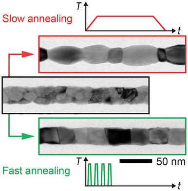
Recent surge in demand for computational power combined with strict constraints on energy consumption requires persistent increase in the density of transistors and memory cells in integrated circuits. Metal interconnects in their current form struggle to follow the size downscaling due to materials limitations at the nanoscale, causing severe performance losses. Next‐generation interconnects need new materials, and molybdenum (Mo) is considered the best choice, offering low resistivity, good scalability, and barrierless integration at a low cost. However, it requires annealing at temperatures far exceeding the currently accepted limit. In this work, the challenges of high‐temperature annealing of patterned Mo nanowires are looked into, and a new approach is presented to overcome them. It is demonstrated that while a conventional annealing process improves the average grain size, it can also reduce the cross‐section area, thus increasing the resistivity. Using high‐resolution transmission electron microscopy (TEM) with in situ heating, the evolution of structural features in real time is directly observed. Using insights from these experiments, a cyclic pulsed annealing method is developed, and it is shown that the desired grain structure is achieved in only a few seconds, without forming the surface grooves. These findings can radically facilitate Mo integration, boosting the efficiency of future integrated circuits.
中文翻译:

解决下一代集成电路钼互连的退火问题
最近对计算能力的需求激增,加上对能耗的严格限制,要求集成电路中晶体管和存储单元的密度持续增加。由于纳米级材料的限制,目前形式的金属互连很难跟随尺寸缩小,导致严重的性能损失。下一代互连需要新材料,而钼 (Mo) 被认为是最佳选择,它具有低电阻率、良好的可扩展性和低成本的无障碍集成。然而,它需要在远远超过目前可接受的极限的温度下进行退火。在这项工作中,研究了图案化钼纳米线高温退火的挑战,并提出了一种新的方法来克服这些挑战。结果表明,传统的退火工艺在提高平均晶粒尺寸的同时,还可以减小横截面积,从而增加电阻率。使用高分辨率透射电子显微镜(TEM)和原位加热,可以直接观察实时结构特征的演变。利用这些实验的见解,开发了一种循环脉冲退火方法,结果表明,只需几秒钟即可实现所需的晶粒结构,而不会形成表面凹槽。这些发现可以从根本上促进钼集成,提高未来集成电路的效率。
更新日期:2024-06-24
中文翻译:
解决下一代集成电路钼互连的退火问题
最近对计算能力的需求激增,加上对能耗的严格限制,要求集成电路中晶体管和存储单元的密度持续增加。由于纳米级材料的限制,目前形式的金属互连很难跟随尺寸缩小,导致严重的性能损失。下一代互连需要新材料,而钼 (Mo) 被认为是最佳选择,它具有低电阻率、良好的可扩展性和低成本的无障碍集成。然而,它需要在远远超过目前可接受的极限的温度下进行退火。在这项工作中,研究了图案化钼纳米线高温退火的挑战,并提出了一种新的方法来克服这些挑战。结果表明,传统的退火工艺在提高平均晶粒尺寸的同时,还可以减小横截面积,从而增加电阻率。使用高分辨率透射电子显微镜(TEM)和原位加热,可以直接观察实时结构特征的演变。利用这些实验的见解,开发了一种循环脉冲退火方法,结果表明,只需几秒钟即可实现所需的晶粒结构,而不会形成表面凹槽。这些发现可以从根本上促进钼集成,提高未来集成电路的效率。


 京公网安备 11010802027423号