Frontiers of Physics ( IF 6.5 ) Pub Date : 2024-06-24 , DOI: 10.1007/s11467-024-1404-9 Chang Lu , Shunhui Zhang , Meili Chen , Haitao Chen , Mengjian Zhu , Zhengwei Zhang , Jun He , Lin Zhang , Xiaoming Yuan
|
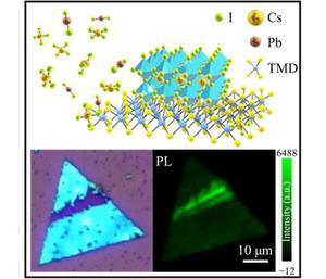
Van der Waals epitaxy allows heterostructure formation without considering the lattice match requirement, thus is a promising method to form 2D/2D and 2D/3D heterojunction. Considering the unique optical properties of CsPbI3 and transition metal dichalcogenides (TMDCs), their heterostructure presents potential applications in both photonics and optoelectronics fields. Here, we demonstrate selective growth of cubic phase CsPbI3 nanofilm with thickness as thin as 4.0 nm and zigzag/armchair oriented nanowires (NWs) on monolayer WSe2. Furthermore, we show growth of CsPbI3 on both transferred WSe2 on copper grid and WSe2–based optoelectrical devices, providing a platform for structure analysis and device performance modification. Transmission electron microscopy (TEM) results reveal the epitaxial nature of cubic CsPbI3 phase. The revealed growth fundamental of CsPbI3 is universal valid for other two-dimensional substrates, offering a great advantage to fabricate CsPbI3 based van der Waals heterostructures (vdWHs). X-ray photoelectron spectroscopy (XPS) and optical characterization confirm the type-II band alignment, resulting in a fast charge transfer process and the occurrence of a broad emission peak at lower energy. The formation of WSe2/CsPbI3 heterostructure largely enhances the photocurrent from 2.38 nA to 38.59 nA. These findings are vital for bottom-up epitaxy of inorganic semiconductor on atomic thin 2D substrates for optoelectronic applications.
中文翻译:
用于光电应用的 II 型能带排列 CsPbI3/TMDC 异质结构的范德华外延
范德华外延可以在不考虑晶格匹配要求的情况下形成异质结构,因此是形成2D/2D和2D/3D异质结的有前途的方法。考虑到CsPbI 3 和过渡金属二硫属化物(TMDC)独特的光学性质,它们的异质结构在光子学和光电子领域具有潜在的应用前景。在这里,我们展示了在单层 WSe 2 上选择性生长厚度薄至 4.0 nm 的立方相 CsPbI 3 纳米薄膜和锯齿形/扶手椅取向纳米线(NW)。此外,我们还展示了 CsPbI 3 在铜栅上转移的 WSe 2 和基于 WSe 2 的光电器件上的生长,为结构分析和器件提供了平台。性能修改。透射电子显微镜 (TEM) 结果揭示了立方 CsPbI 3 相的外延性质。所揭示的 CsPbI 3 生长原理对于其他二维基底普遍有效,为制造基于 CsPbI 3 的范德华异质结构(vdWH)提供了巨大的优势。 X 射线光电子能谱 (XPS) 和光学表征证实了 II 型能带排列,从而导致快速电荷转移过程并在较低能量下出现宽发射峰。 WSe 2 /CsPbI 3 异质结构的形成大大提高了光电流从2.38 nA到38.59 nA。这些发现对于光电应用的原子薄二维基板上的无机半导体自下而上外延至关重要。


 京公网安备 11010802027423号