当前位置:
X-MOL 学术
›
Adv. Electron. Mater.
›
论文详情
Our official English website, www.x-mol.net, welcomes your feedback! (Note: you will need to create a separate account there.)
Analysis and EOT Scaling on Top‐ and Double‐Gate 2D CVD‐Grown Monolayer MoS2 FETs
Advanced Electronic Materials ( IF 5.3 ) Pub Date : 2024-06-22 , DOI: 10.1002/aelm.202400152 Naim Hossain Patoary 1 , Fahad Al Mamun 1 , Jing Xie 1 , Tibor Grasser 2 , Ivan Sanchez Esqueda 1
Advanced Electronic Materials ( IF 5.3 ) Pub Date : 2024-06-22 , DOI: 10.1002/aelm.202400152 Naim Hossain Patoary 1 , Fahad Al Mamun 1 , Jing Xie 1 , Tibor Grasser 2 , Ivan Sanchez Esqueda 1
Affiliation
|
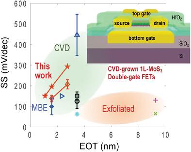
2D layered semiconductors have attracted considerable attention for beyond‐Si complementary metal‐oxide‐semiconductor (CMOS) technologies. They can be prepared into ultrathin channel materials toward ultrascaled device architectures, including double‐gate field‐effect‐transistors (DGFETs). This work presents an experimental analysis of DGFETs constructed from chemical vapor deposition (CVD)‐grown monolayer (1L) molybdenum disulfide (MoS2 ) with atomic layer deposition (ALD) of hafnium oxide (HfO2 ) high‐k gate dielectrics (top and bottom). This extends beyond previous studies of DGFETs based mostly on exfoliated (few‐nm thick) MoS2 flakes, and advances toward large‐area wafer‐scale processing. Here, significant improvements in performance are obtained with DGFETs (i.e., improvements in ON/OFF ratio, ON‐state current, sub‐threshold swing, etc.) compared to single top‐gate FETs. In addition to multi‐gate device architectures (e.g., DGFETs), the scaling of the equivalent oxide thickness (EOT) is crucial toward improved electrostatics required for next‐generation transistors. However, the impact of EOT scaling on the characteristics of CVD‐grown MoS2 DGFETs remains largely unexplored. Thus, this work studies the impact of EOT scaling on subthreshold swing (SS) and gate hysteresis using current–voltage (I–V ) measurements with varying sweep rates. The experimental analysis and results elucidate the basic mechanisms responsible for improvements in CVD‐grown 1L‐MoS2 DGFETs compared to standard top‐gate FETs.
中文翻译:

顶栅和双栅 2D CVD 生长单层 MoS2 FET 的分析和 EOT 缩放
二维层状半导体对于超硅互补金属氧化物半导体(CMOS)技术引起了广泛关注。它们可以制备成超薄沟道材料,用于超大规模器件架构,包括双栅场效应晶体管(DGFET)。这项工作对由化学气相沉积 (CVD) 生长的单层 (1L) 二硫化钼 (MoS2) 和氧化铪 (HfO2) 高 k 栅极电介质原子层沉积 (ALD) 构建的 DGFET 进行了实验分析(顶部和底部) 。这超出了之前主要基于剥离(几纳米厚)MoS2 薄片的 DGFET 的研究,并向大面积晶圆级加工迈进。在这里,与单顶栅 FET 相比,DGFET 的性能得到了显着改进(即开/关比、导通状态电流、亚阈值摆幅等方面的改进)。除了多栅极器件架构(例如 DGFET)之外,等效氧化物厚度(EOT)的缩放对于改善下一代晶体管所需的静电性能至关重要。然而,EOT 缩放对 CVD 生长的 MoS2 DGFET 特性的影响在很大程度上仍未得到探索。因此,这项工作使用不同扫描速率的电流-电压 (I-V) 测量来研究 EOT 缩放对亚阈值摆幅 (SS) 和栅极磁滞的影响。实验分析和结果阐明了 CVD 生长的 1L-MoS2 DGFET 与标准顶栅 FET 相比改进的基本机制。
更新日期:2024-06-22
中文翻译:
顶栅和双栅 2D CVD 生长单层 MoS2 FET 的分析和 EOT 缩放
二维层状半导体对于超硅互补金属氧化物半导体(CMOS)技术引起了广泛关注。它们可以制备成超薄沟道材料,用于超大规模器件架构,包括双栅场效应晶体管(DGFET)。这项工作对由化学气相沉积 (CVD) 生长的单层 (1L) 二硫化钼 (MoS2) 和氧化铪 (HfO2) 高 k 栅极电介质原子层沉积 (ALD) 构建的 DGFET 进行了实验分析(顶部和底部) 。这超出了之前主要基于剥离(几纳米厚)MoS2 薄片的 DGFET 的研究,并向大面积晶圆级加工迈进。在这里,与单顶栅 FET 相比,DGFET 的性能得到了显着改进(即开/关比、导通状态电流、亚阈值摆幅等方面的改进)。除了多栅极器件架构(例如 DGFET)之外,等效氧化物厚度(EOT)的缩放对于改善下一代晶体管所需的静电性能至关重要。然而,EOT 缩放对 CVD 生长的 MoS2 DGFET 特性的影响在很大程度上仍未得到探索。因此,这项工作使用不同扫描速率的电流-电压 (I-V) 测量来研究 EOT 缩放对亚阈值摆幅 (SS) 和栅极磁滞的影响。实验分析和结果阐明了 CVD 生长的 1L-MoS2 DGFET 与标准顶栅 FET 相比改进的基本机制。


 京公网安备 11010802027423号