当前位置:
X-MOL 学术
›
J. Am. Chem. Soc.
›
论文详情
Our official English website, www.x-mol.net, welcomes your
feedback! (Note: you will need to create a separate account there.)
Mono-, Few-, and Multiple Layers of Copper Antimony Sulfide (CuSbS2): A Ternary Layered Sulfide
Journal of the American Chemical Society ( IF 14.4 ) Pub Date : 2014-01-15 , DOI: 10.1021/ja411748g Karthik Ramasamy 1 , Hunter Sims 1 , William H. Butler 1 , Arunava Gupta 1
Journal of the American Chemical Society ( IF 14.4 ) Pub Date : 2014-01-15 , DOI: 10.1021/ja411748g Karthik Ramasamy 1 , Hunter Sims 1 , William H. Butler 1 , Arunava Gupta 1
Affiliation
|
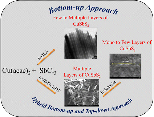
Layered materials with controlled thickness down to monolayer are being intensively investigated for unraveling and harnessing their dimension-dependent properties. Copper antimony sulfide (CuSbS2) is a ternary layered semiconductor material that has been considered as an absorber material in thin film solar cells due to its optimal band gap (∼1.5 eV) with high absorption coefficient of over >10(4) cm(-1). We have for the first time developed solution-based approaches for the synthesis of mono-, few-, and multiple layers of CuSbS2. These include a colloidal bottom-up approach for the synthesis of CuSbS2 nanoplates with thicknesses from six layers to several layers, and a hybrid bottom-up-top-down approach for the formation of CuSbS2 mesobelts. The latter can be exfoliated by Li-ion intercalation and sonication to obtain layers down to monolayer thickness. Time-dependent TEM studies provide important insights into the growth mechanism of mesobelts. At the initial stage the nanoplates grow laterally to form nanosheets as the primary structure, followed by their folding and attachment through homoepitaxy to form prolate-like secondary structures. Eventually, these prolate-like structures form mesocrystals by oriented attachment crystal growth. The changes in optical properties with layer thickness down to monolayers have been studied. In order to understand the thickness-dependent optical and electrical properties, we have calculated the electronic structures of mono- and multiple layers (bulk) of CuSbS2 using the hybrid functional method (HSE 06). We find that the monolayers exhibit noticeably different properties from the multilayered or the bulk system, with a markedly increased band gap that is, however, compromised by the presence of localized surface states. These localized states are predominantly composed of energetically favorable Sb pz states, which break off from the rest of the Sb p states that would otherwise be at the top of the gap. The developed solution-based synthesis approaches are versatile and can likely be extended to other complex layered sulfides.
中文翻译:

单层、少层和多层铜硫化锑 (CuSbS2):三元层状硫化物
正在深入研究具有受控厚度到单层的层状材料,以揭示和利用其与尺寸相关的特性。铜硫化锑 (CuSbS2) 是一种三元层状半导体材料,由于其最佳带隙 (~1.5 eV) 和超过 >10(4) cm(- 1)。我们首次开发了基于溶液的方法来合成单层、少层和多层 CuSbS2。其中包括用于合成厚度从六层到几层的 CuSbS2 纳米板的胶体自下而上的方法,以及用于形成 CuSbS2 中间带的自下而上自上而下的混合方法。后者可以通过锂离子嵌入和超声处理剥离,以获得低至单层厚度的层。瞬态 TEM 研究提供了对中带生长机制的重要见解。在初始阶段,纳米板横向生长以形成纳米片作为一级结构,然后通过同质外延折叠和附着形成长条状二级结构。最终,这些长条状结构通过定向附着晶体生长形成中间晶体。已经研究了随着层厚度下降到单层的光学特性的变化。为了了解厚度相关的光学和电学特性,我们使用混合功能方法 (HSE 06) 计算了 CuSbS2 的单层和多层(体)的电子结构。我们发现单层表现出与多层或体系统明显不同的特性,带隙显着增加,但是由于局部表面状态的存在而受到损害。这些局部状态主要由能量上有利的 Sb pz 状态组成,这些状态与其余的 Sb p 状态分开,否则这些状态将位于间隙顶部。开发的基于溶液的合成方法是通用的,可能会扩展到其他复杂的层状硫化物。它与其余的 Sb p 状态分开,否则这些状态将处于间隙的顶部。开发的基于溶液的合成方法是通用的,可能会扩展到其他复杂的层状硫化物。它与其余的 Sb p 状态分开,否则这些状态将处于间隙的顶部。开发的基于溶液的合成方法是通用的,可能会扩展到其他复杂的层状硫化物。
更新日期:2014-01-15
中文翻译:
单层、少层和多层铜硫化锑 (CuSbS2):三元层状硫化物
正在深入研究具有受控厚度到单层的层状材料,以揭示和利用其与尺寸相关的特性。铜硫化锑 (CuSbS2) 是一种三元层状半导体材料,由于其最佳带隙 (~1.5 eV) 和超过 >10(4) cm(- 1)。我们首次开发了基于溶液的方法来合成单层、少层和多层 CuSbS2。其中包括用于合成厚度从六层到几层的 CuSbS2 纳米板的胶体自下而上的方法,以及用于形成 CuSbS2 中间带的自下而上自上而下的混合方法。后者可以通过锂离子嵌入和超声处理剥离,以获得低至单层厚度的层。瞬态 TEM 研究提供了对中带生长机制的重要见解。在初始阶段,纳米板横向生长以形成纳米片作为一级结构,然后通过同质外延折叠和附着形成长条状二级结构。最终,这些长条状结构通过定向附着晶体生长形成中间晶体。已经研究了随着层厚度下降到单层的光学特性的变化。为了了解厚度相关的光学和电学特性,我们使用混合功能方法 (HSE 06) 计算了 CuSbS2 的单层和多层(体)的电子结构。我们发现单层表现出与多层或体系统明显不同的特性,带隙显着增加,但是由于局部表面状态的存在而受到损害。这些局部状态主要由能量上有利的 Sb pz 状态组成,这些状态与其余的 Sb p 状态分开,否则这些状态将位于间隙顶部。开发的基于溶液的合成方法是通用的,可能会扩展到其他复杂的层状硫化物。它与其余的 Sb p 状态分开,否则这些状态将处于间隙的顶部。开发的基于溶液的合成方法是通用的,可能会扩展到其他复杂的层状硫化物。它与其余的 Sb p 状态分开,否则这些状态将处于间隙的顶部。开发的基于溶液的合成方法是通用的,可能会扩展到其他复杂的层状硫化物。


 京公网安备 11010802027423号