当前位置:
X-MOL 学术
›
J. Phys. Chem. C
›
论文详情
Our official English website, www.x-mol.net, welcomes your feedback! (Note: you will need to create a separate account there.)
Crystal and Electronic Structures of Epitaxial Atomic Thick Lead Iodide
The Journal of Physical Chemistry C ( IF 3.3 ) Pub Date : 2024-06-20 , DOI: 10.1021/acs.jpcc.4c01471 Qi Wang 1 , Li-Ying Zhang 2 , Zhibo Yuan 1 , Ye-Heng Song 1, 3 , Yu Jia 2 , Weifeng Zhang 1, 3
The Journal of Physical Chemistry C ( IF 3.3 ) Pub Date : 2024-06-20 , DOI: 10.1021/acs.jpcc.4c01471 Qi Wang 1 , Li-Ying Zhang 2 , Zhibo Yuan 1 , Ye-Heng Song 1, 3 , Yu Jia 2 , Weifeng Zhang 1, 3
Affiliation
|
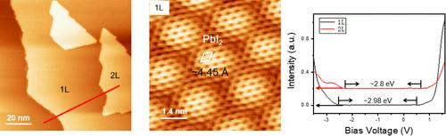
Lead iodide (PbI2), a typical layered semiconductor material, holds a wide visible band gap and a thickness-dependent band structure, which can be widely used in optical devices and perovskite solar cells. Although lead iodide is one of the most extensively studied materials, there is still a lack of experimental investigation of the electrical structure. In this study, we successfully grow the PbI2 monolayer on the highly oriented pyrolytic graphite (HOPG) substrate by molecular beam epitaxy (MBE). Scanning tunneling microscopy (STM) characterization demonstrates the high-quality PbI2 monolayer with a distinct Moiré pattern. Spectroscopic measurements reveal that the PbI2 monolayer possesses a band gap of ∼2.98 eV in the visible purple range and a decreased band gap of ∼2.8 eV for the bilayer. Theoretical calculations corroborate the experiments and reveal an indirect-to-direct bandgap transition in the bilayer. This study has significant implications for the future field of optical devices.
中文翻译:

外延原子厚碘化铅的晶体和电子结构
碘化铅(PbI 2 )是一种典型的层状半导体材料,具有较宽的可见带隙和厚度相关的能带结构,可广泛应用于光学器件和钙钛矿太阳能电池。尽管碘化铅是研究最广泛的材料之一,但仍然缺乏对其电结构的实验研究。在本研究中,我们通过分子束外延(MBE)成功在高取向热解石墨(HOPG)基板上生长了PbI 2 单层。扫描隧道显微镜 (STM) 表征表明高质量的 PbI 2 单层具有独特的莫尔图案。光谱测量表明,PbI 2 单层在可见紫色范围内具有~2.98 eV 的带隙,而双层的带隙则减小了~2.8 eV。理论计算证实了实验并揭示了双层中间接到直接带隙的转变。这项研究对未来的光学器件领域具有重要意义。
更新日期:2024-06-21
中文翻译:
外延原子厚碘化铅的晶体和电子结构
碘化铅(PbI 2 )是一种典型的层状半导体材料,具有较宽的可见带隙和厚度相关的能带结构,可广泛应用于光学器件和钙钛矿太阳能电池。尽管碘化铅是研究最广泛的材料之一,但仍然缺乏对其电结构的实验研究。在本研究中,我们通过分子束外延(MBE)成功在高取向热解石墨(HOPG)基板上生长了PbI 2 单层。扫描隧道显微镜 (STM) 表征表明高质量的 PbI 2 单层具有独特的莫尔图案。光谱测量表明,PbI 2 单层在可见紫色范围内具有~2.98 eV 的带隙,而双层的带隙则减小了~2.8 eV。理论计算证实了实验并揭示了双层中间接到直接带隙的转变。这项研究对未来的光学器件领域具有重要意义。


 京公网安备 11010802027423号