Nature Nanotechnology ( IF 38.1 ) Pub Date : 2024-06-21 , DOI: 10.1038/s41565-024-01693-3 Yu-Cheng Lu , Jing-Kai Huang , Kai-Yuan Chao , Lain-Jong Li , Vita Pi-Ho Hu
|
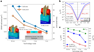
Researchers have been developing 2D materials (2DM) for electronics, which are widely considered a possible replacement for silicon in future technology. Two-dimensional transition metal dichalcogenides are the most promising among the different materials due to their electronic performance and relatively advanced development. Although field-effect transistors (FETs) based on 2D transition metal dichalcogenides have been found to outperform Si in ultrascaled devices, the comparison of 2DM-based and Si-based technologies at the circuit level is still missing. Here we compare 2DM- and Si FET-based static random-access memory (SRAM) circuits across various technology nodes from 16 nm to 1 nm and reveal that the 2DM-based SRAM exhibits superior performance in terms of stability, operating speed and energy efficiency when compared with Si SRAM. This study utilized technology computer-aided design to conduct device and circuit simulations, employing calibrated MoS2 nFETs and WSe2 pFETs. It incorporated layout design rules across various technology nodes to comprehensively analyse their SRAM functionality. The results show that, compared with three-dimensional structure Si transistors at 1 nm node, the planar 2DMFETs exhibited lower capacitance, leading to reduced cell read access time (−16%), reduced time to write (−72%) and lowered dynamic power (−60%). The study highlights the provisional benefits of using planar 2DM transistors to mitigate the performance degradation caused by reduced metal pitch and increased wire resistance in advanced nodes, potentially opening up exciting possibilities for high-performance and low-power circuit applications.
中文翻译:
基于硅和二维材料的 SRAM 电路的预计性能范围从 16nm 到 1nm 技术节点
研究人员一直在开发用于电子产品的二维材料(2DM),这种材料被广泛认为是未来技术中硅的可能替代品。二维过渡金属二硫属化物由于其电子性能和相对先进的发展而成为各种材料中最有前途的。尽管基于 2D 过渡金属二硫族化物的场效应晶体管 (FET) 在超大规模器件中的性能优于 Si,但仍缺乏在电路层面对基于 2DM 和基于 Si 的技术进行比较。在这里,我们比较了 16 nm 至 1 nm 不同技术节点的基于 2DM 和 Si FET 的静态随机存取存储器 (SRAM) 电路,发现基于 2DM 的 SRAM 在稳定性、运行速度和能效方面表现出卓越的性能与 Si SRAM 相比。本研究利用计算机辅助设计技术进行器件和电路模拟,采用校准的 MoS 2 nFET 和 WSe 2 pFET。它结合了跨各种技术节点的布局设计规则,以全面分析其 SRAM 功能。结果表明,与 1 nm 节点的三维结构 Si 晶体管相比,平面 2DMFET 表现出较低的电容,从而减少了单元读取访问时间 (-16%)、写入时间 (-72%) 并降低了动态性能功率(−60%)。该研究强调了使用平面 2DM 晶体管来缓解先进节点中因金属间距减小和导线电阻增加而导致的性能下降的暂时优势,这可能为高性能和低功耗电路应用带来令人兴奋的可能性。


 京公网安备 11010802027423号