当前位置:
X-MOL 学术
›
ACS Photonics
›
论文详情
Our official English website, www.x-mol.net, welcomes your feedback! (Note: you will need to create a separate account there.)
Monolayer Semiconductor Superlattices with High Optical Absorption
ACS Photonics ( IF 6.5 ) Pub Date : 2024-06-17 , DOI: 10.1021/acsphotonics.4c00277 Sara A. Elrafei 1 , Lennart M. Heijnen 1 , Rasmus H. Godiksen 1 , Alberto G. Curto 1, 2, 3
ACS Photonics ( IF 6.5 ) Pub Date : 2024-06-17 , DOI: 10.1021/acsphotonics.4c00277 Sara A. Elrafei 1 , Lennart M. Heijnen 1 , Rasmus H. Godiksen 1 , Alberto G. Curto 1, 2, 3
Affiliation
|
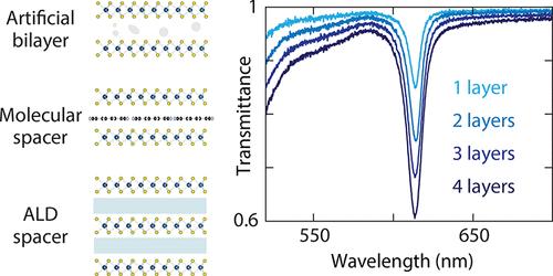
Optical absorption plays a central role in optoelectronic and photonic technologies. Strongly absorbing materials are thus needed for efficient and miniaturized devices. A uniform film much thinner than the wavelength can only absorb up to 50% of the incident light when embedded in a symmetric and homogeneous environment. Although deviating from these conditions allows higher absorption, finding the thinnest possible material with the highest intrinsic absorption is still desirable. Here, we demonstrate strong absorption by artificially stacking WS2 monolayers into superlattices. We compare three simple approaches based on different spacer materials to surpass the peak absorptance of a single WS2 monolayer, which stands at 16% on ideal substrates. Through direct monolayer stacking without an intentional spacer, we reach an absorptance of 27% for an artificial bilayer, although with limited control over interlayer distance. Using a molecular spacer via spin coating, we demonstrate controllable spacer thickness in a bilayer with 25% absorptance while increasing photoluminescence thanks to doping. Finally, we exploit the atomic layer deposition of alumina spacers to boost the absorptance to 31% for a 4-monolayer superlattice. Our results demonstrate that monolayer superlattices are a powerful platform directly applicable to improve strong light-matter coupling and enhance the performance of nanophotonic devices such as modulators and photodetectors.
中文翻译:

具有高光吸收的单层半导体超晶格
光吸收在光电和光子技术中起着核心作用。因此,高效和小型化的设备需要强吸收材料。当嵌入对称且均匀的环境中时,比波长薄得多的均匀薄膜最多只能吸收 50% 的入射光。尽管偏离这些条件可以实现更高的吸收,但仍然需要找到具有最高本征吸收的最薄的材料。在这里,我们通过人工将 WS 2 单层堆叠到超晶格中来证明强吸收。我们比较了基于不同间隔材料的三种简单方法,以超过单个 WS 2 单层的峰值吸收率,该峰值吸收率在理想基材上为 16%。通过直接单层堆叠而不使用有意的间隔物,我们实现了人造双层的 27% 的吸收率,尽管对层间距离的控制有限。通过旋涂使用分子间隔物,我们展示了具有 25% 吸收率的双层中可控的间隔物厚度,同时通过掺杂增加了光致发光。最后,我们利用氧化铝间隔物的原子层沉积将 4 单层超晶格的吸收率提高到 31%。我们的结果表明,单层超晶格是一个强大的平台,可直接用于改善强光-物质耦合并增强调制器和光电探测器等纳米光子器件的性能。
更新日期:2024-06-18
中文翻译:
具有高光吸收的单层半导体超晶格
光吸收在光电和光子技术中起着核心作用。因此,高效和小型化的设备需要强吸收材料。当嵌入对称且均匀的环境中时,比波长薄得多的均匀薄膜最多只能吸收 50% 的入射光。尽管偏离这些条件可以实现更高的吸收,但仍然需要找到具有最高本征吸收的最薄的材料。在这里,我们通过人工将 WS 2 单层堆叠到超晶格中来证明强吸收。我们比较了基于不同间隔材料的三种简单方法,以超过单个 WS 2 单层的峰值吸收率,该峰值吸收率在理想基材上为 16%。通过直接单层堆叠而不使用有意的间隔物,我们实现了人造双层的 27% 的吸收率,尽管对层间距离的控制有限。通过旋涂使用分子间隔物,我们展示了具有 25% 吸收率的双层中可控的间隔物厚度,同时通过掺杂增加了光致发光。最后,我们利用氧化铝间隔物的原子层沉积将 4 单层超晶格的吸收率提高到 31%。我们的结果表明,单层超晶格是一个强大的平台,可直接用于改善强光-物质耦合并增强调制器和光电探测器等纳米光子器件的性能。


 京公网安备 11010802027423号