Nature Materials ( IF 37.2 ) Pub Date : 2024-05-13 , DOI: 10.1038/s41563-024-01894-0 Laisi Chen 1 , Amy X Wu 1 , Naol Tulu 1 , Joshua Wang 1 , Adrian Juanson 2 , Kenji Watanabe 3 , Takashi Taniguchi 4 , Michael T Pettes 5 , Marshall A Campbell 1, 5 , Mingjie Xu 6 , Chaitanya A Gadre 1 , Yinong Zhou 1 , Hangman Chen 7 , Penghui Cao 7 , Luis A Jauregui 1 , Ruqian Wu 1 , Xiaoqing Pan 1, 6, 8 , Javier D Sanchez-Yamagishi 1
|
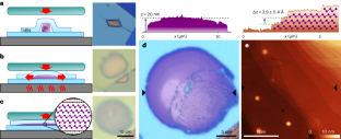
Confining materials to two-dimensional forms changes the behaviour of the electrons and enables the creation of new devices. However, most materials are challenging to produce as uniform, thin crystals. Here we present a synthesis approach where thin crystals are grown in a nanoscale mould defined by atomically flat van der Waals (vdW) materials. By heating and compressing bismuth in a vdW mould made of hexagonal boron nitride, we grow ultraflat bismuth crystals less than 10 nm thick. Due to quantum confinement, the bismuth bulk states are gapped, isolating intrinsic Rashba surface states for transport studies. The vdW-moulded bismuth shows exceptional electronic transport, enabling the observation of Shubnikov–de Haas quantum oscillations originating from the (111) surface state Landau levels. By measuring the gate-dependent magnetoresistance, we observe multi-carrier quantum oscillations and Landau level splitting, with features originating from both the top and bottom surfaces. Our vdW mould growth technique establishes a platform for electronic studies and control of bismuth’s Rashba surface states and topological boundary modes1,2,3. Beyond bismuth, the vdW-moulding approach provides a low-cost way to synthesize ultrathin crystals and directly integrate them into a vdW heterostructure.
中文翻译:
范德华材料内生长的薄铋晶体具有出色的电子传输和量子振荡
将材料限制为二维形式可以改变电子的行为并能够创建新设备。然而,大多数材料很难生产出均匀、薄的晶体。在这里,我们提出了一种合成方法,其中薄晶体在由原子级平坦范德华(vdW)材料定义的纳米级模具中生长。通过在由六方氮化硼制成的 vdW 模具中加热和压缩铋,我们生长出厚度小于 10 nm 的超扁平铋晶体。由于量子限制,铋体态存在间隙,从而隔离了本征 Rashba 表面态以用于输运研究。 vdW 模制铋显示出出色的电子传输,使得能够观察源自 (111) 表面态朗道能级的舒布尼科夫-德哈斯量子振荡。通过测量与栅极相关的磁阻,我们观察到多载流子量子振荡和朗道能级分裂,其特征源自顶面和底面。我们的 vdW 模具生长技术为铋的 Rashba 表面态和拓扑边界模式的电子研究和控制建立了一个平台1,2,3 。除了铋之外,vdW 成型方法还提供了一种低成本的方法来合成超薄晶体并将其直接集成到 vdW 异质结构中。


 京公网安备 11010802027423号